


This version (11 Oct 2022 14:05) was approved by Shine Cabatan.The Previously approved version (12 Aug 2022 12:03) is available.
Table of Contents
EVALUATING THE AD9135/AD9136 DIGITAL-TO-ANALOG CONVERTER
Preface
This user guide describes both the hardware and software setup needed to acquire data capture from AD9135-FMC-EBZ/AD9136-FMC-EBZ evaluation board to characterize AD9135/AD9136 11-/16-bit 2.8Gsps dual JESD204B signal processing RF Digital to Analog Converter.
The AD9135-FMC-EBZ/AD9136-FMC-EBZ is an FMC mezzanine card and connects to an ADS7-V2 or ADS8-V1 data pattern generator system. The ADS7-V2/ADS8-V1 automatically formats the data and sends it to the AD9135/AD9136 FMC card via its JESD204B lanes. +12V, +3.3V, and VADJ power supply rails are provided by the ADS7-V2/ADS8-V1 system via the FMC connector P1. A clock distribution chip AD9516 is included on this EVB as a clock fan-out and frequency divider for the DACCLK, JESD204B SYSREF signals, and a GBTCLK clock used by the ADS7-V2/ADS8-V1. There is also an FMC standard I2C bus that is used by the ADS7-V2/ADS8-V1 to identify the AD9135/AD9136 FMC card. This I2C interface is implemented in software in the AD9135/AD9136 FMC card PIC processor (XU1). All ADS7-V2/ADS8-V1 to/from AD9135/AD9136 FMC card interface signals are connected via the FMC connector P1.
Typical Setup
 Figure 1a. AD9135-FMC-EBZ Setup with ADS7-V2EBZ
 Figure 1b. AD9135-FMC-EBZ Setup with ADS8-V1EBZ
 Figure 2a. AD9136-FMC-EBZ Setup with ADS7-V2EBZ
 Figure 2b. AD9136-FMC-EBZ Setup with ADS8-V1EBZ
Tip: Click on any picture in this guide to open an enlarged version.
Helpful Files/Links
- AD9135-EBZ/AD9136-EBZ User Guide for non-FMC card users
- Datasheet: AD9135/AD9136
- AMI Model: AD9144/AD9152/AD9154/AD9135/AD9136
- Simulink ADIsimDAC Model: AD9136
- Schematic: AD9135-FMC-EBZ, AD9136-FMC-EBZ
- Bill of Materials: AD9135-FMC-EBZ, AD9136-FMC-EBZ
- PCB Gerber Files: RevB
- PCB BRD File: RevB
- PCB Layout PDF: RevB
Software Needed
- DPG Lite (Recommended; Installed with ACE) or DPG Downloader
- Do not install ACE on a computer with DAC Software Suite.
- Known Issue: ACE may fail to detect HS-DAC boards, details here.
Hardware Needed
- AD9135-FMC-EBZ/AD9136-FMC-EBZ Evaluation Board which comes with:
- USB-A to USB-Mini Cable
- ADS7-V2EBZ or ADS8-V1EBZ Evaluation Kit which includes:
- 12V 60W AC/DC Power Supply
- Power Cord
- USB-A to USB-B Cable
- PC with ACE and DPG Lite Software Applications
- Low Phase Noise High-Frequency Continuous Wave Generator
- Signal/Spectrum Analyzer and/or Wide Bandwidth Oscilloscope
- (3) SMA Cables
Quick Start Guide
- Attach AD9135-FMC-EBZ/AD9136-FMC-EBZ onto the FMC connector of ADS7-V2 or ADS8-V1 controller board. Connect the evaluation board to PC via USB, the continuous waveform generator output to J1, the DAC output at J17 to a signal/spectrum analyzer, and, if desired, the other DAC output at J5 to an oscilloscope. Connect ADS7-V2/ADS8-V1 to PC via USB and to a 12V 60W AC/DC power supply, then switch the board ON using S1 beside the connector for 12V supply. Refer to Typical Setup section for pictures of actual evaluation setup.
- Set the frequency of the continuous waveform generator output to 2.0 GHz and the output level to +3 dBm. Enable the output.
 Figure 3. ADS7-V2 and AD9136 detected in DPG Software
- Start DPG Lite or DPG Downloader. A panel named after the detected controller board should appear at the bottom of the DPG window. The device on the evaluation board and the data interface should also be automatically detected by the software and shown at Evaluation Board and Port Configuration, respectively.
 Figure 4. AD9136-FMC-EBZ detected in ACE
- Open ACE. The board will automatically be recognized by the software. Otherwise, install the plugin for AD9135/AD9136 evaluation board by following the steps in this page: Quickstart - ACE Quickstart and Plug-in Installation.
 Figure 5. ACE Initial Configuration Wizard
 Figure 6. ACE AD9136 Chipview Tab
- In ACE, apply the configuration wizard settings enumerated below and shown in Figure 5. JESD204B PLL should lock and the indicator should turn green.
- Links: Dual Link
- JESD Mode: 8
- Subclass1: True
- Interpolation: 1
- DAC PLL: False
- FDAC: 2 GHz
 Figure 7. Single Tone and ADS7-V2 Configuration Panels in DPG
- In DPG Lite or DPG Downloader, configure generation of two single tone waveforms. From the Add Generator Waveforms pulldown menu, select Single Tone. Do this two times then configure the panels as follows:
- Data Rate = 2 GHz, Amplitude = -1dBFS, Unsigned Data is unchecked for both panels.
- Desired Frequency = 112 MHz in one panel while Desired Frequency = 221 MHz in the other.
- If using AD9135, set DAC Resolution to 11 bits. Otherwise, leave as is (16 bits).
- In the ADS7-V2 or ADS8-V1 panel in the DPG window, configure Data Playback by selecting tone2 for DAC0 and tone1 for DAC1. Set JESD Mode to Mode 8, Links to Dual, and Subclass to 1.
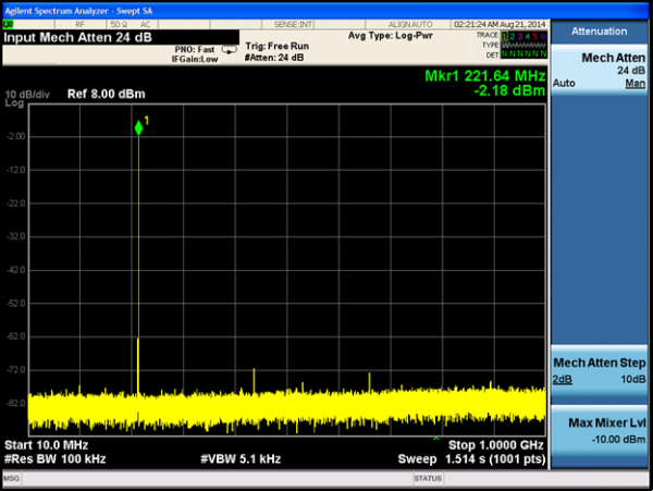 Figure 8. DAC0 Output Spectrum Analyzer Display
 Figure 9. DAC1 Output Scope Display
- Press the download arrow (
 ) then the play button (
 ). Serial Line Rate should appear as 10 Gbps and Sync Status should have two check marks. Refer to FFT plot of the DAC0 output in Figure 8 and the oscilloscope capture of DAC1 output in Figure 9.


resources/eval/dpg/ad9136-fmc-ebz.txt · Last modified: 11 Oct 2022 14:05 by Shine Cabatan