


This version (22 Mar 2021 10:11) was approved by Michael Hennerich.The Previously approved version (18 Mar 2021 16:24) is available.
Table of Contents
JESD204 Eye Scan
About
The combination of increasing JESD204B serial line rates and PCB based attenuation and distortion increasing, the quality and correctness of differential pair at a JESD204B receiver becomes questionable. The combination of the bit sampling time decreasing (as speed increases), and channel attenuation increasing (as speed increases) both negatively impact the data recovery from the received serial data stream.
This poses a challenge in most designs to system bring-up and release to production because the quality of the line cannot be determined by measuring the far-end eye opening at the receiver pins with readily available lab equipment. Not only does this require prohibitively expensive equipment 1), or it becomes impossible, as the received eye measured on the printed circuit board can appear to be completely closed.
How is anyone supposed to release a product to manufacturing when they don't know if the 10 prototypes that are working are accidentally successful or if they have plenty of design margin?
FPGA Hardware
Luckily, the problem of verifying high speed transceiver performance was solved by the FPGA manufactures years ago, and we can take advantage of the functionality they have added to their chips to determine the overall design margin in a JESD204B solution without purchasing expensive test equipment.
![]()
This illustrates the blocks dedicated to achieving signal integrity in the Xilinx 7-Series FPGA GTP transceivers. All the shaded blocks — PLL, TX pre-emphasis, RX automatic gain control (AGC), RX linear equalization (EQ), RX clock data recovery (CDR), and adaptation block all ensure as robust as link as possible. The 2-D Eye Scan block attached to the receive path provides the functionality of an on-chip scope to visualize post-equalization signal quality in a JESD204B receiver.

As shown above, eye scan runs a separate sampler (figure on the left) which can be adjusted in the horizontal (time) and vertical (amplitude) dimension in parallel with the normal CDR data sampler located in the middle of the horizontal and vertical sale. Xilinx uses this to transfer data over JTAG to create a representative picture on your development host with their IBERT tool.

For each offset setting, the error counter is cleared, and a specified number of bits are transmitted. The data and offset samples are compared bit by bit. When the two samples are not equal, the error counter is incremented. when the specific number of bits are complete, the comparison stops, and bit error rate can be calculated by dividing the error counts by the number of bits transmitted.
This statistically recreates the eye diagram after the equalizer, showing how much design margin is in the system.
BERT Testing
For a 5.0 Gbps link, there are 5,000,000,000 bits per second. This provides a 2 x 10⁻¹⁰ seconds per bit.
In order to measure a BERT rate of 10-10, the system would need to transmit 1010 bits, or 2 seconds of data before it could determine that. As BERT goes up by factors of 10, so must the time.
| BERT Rate | Number of Bits | time to transmit |
|---|---|---|
| 10-8 | 108 | 20 milliseconds |
| 10-9 | 109 | 0.2 seconds |
| 10-10 | 1010 | 2 seconds |
| 10-11 | 1011 | 20 seconds |
| 10-12 | 1012 | 200 seconds, or 3.33 minutes |
| 10-13 | 1013 | 33.33 minutes |
| 10-14 | 1014 | 333.33 minutes, or 5.55 hours |
| 10-15 | 1015 | 55.55 hours, or 2.31 days |
| 10-16 | 1016 | 23.14814815 days, or 3.30 weeks |
| 10-17 | 1017 | 33.06 weeks or ~8 months |
However, this is multiplied by the number of “pixels” (offsets in the time and voltages scales) of the that data. In order to get the most detailed picture, the Xilinx 7 series eye scan supports +/- 32 offsets in the horizontal (time) dimension, and 128 offsets in the vertical (voltage) dimension. This is 8192 (64 x 128) pixels per “frame”. This means it would take 163.84 seconds, or 2.7 minutes (8192 * 20 milliseconds) to capture 10-8 BERT, and 5400+ years to generate the picture at a BERT of 10-17.
Clearly - this isn't practical, so what we attempt to do
Mask
The JESD204B specification outlines an receive keep-out mask based on channel baud rate. To be compliant, the signals at the receiver must stay outside the pre-defined mask area for the baud rate in use.
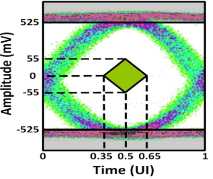
However, this specification is provided in millivolts and time (in unit intervals). As discussed above, the 2-D eye scan operates after the AGC and equalizer blocks inside the FPGA, so it is difficult (impossible) to correlate voltage on the Rx pins of the FPGA, to the vertical axis in the 2-D statistical eye diagram.
The vertical axis in the 2-D statistical eye diagram is in “codes”, not millivolts.
The mask that is shown is not the JESD204B mask, but the Xilinx CDR mask - since this is really the only thing that really matters inside the FPGA.
Software
Overview
The JESD204B eye scan tool that Analog Devices created runs natively on a the ZC706 (under Linux) and creates the pictures below. It does this by using the Xilinx hardware described above, using an HDL/Linux reference design that was created by Analog Devices.
This reference design gathers data directly from the on-chip Receive margin analysis feature in the 7 series IBERT core and manages the data locally inside the FPGA or one of the ARM dual-core Cortex-A9 processors, displaying the data on a HDMI monitor. This measures link robustness using actual JESD204B serial data running from the converter to the FPGA. This use of “live” data enables signal fidelity to be monitored even after the design has been deployed in the field, which allows for real-time and predictive maintenance over the life of the product.
Also see here: JESD204B Status Utility
Source
When building the source code, make sure that gnuplot & libgtk3-dev & required build dependencies are installed.
On Debian/Ubuntu do:
apt-get update
apt-get install -y git build-essential gnuplot libgtk-3-dev libncurses-dev
On CentOS/Redhat
yum update
yum -y groupinstall 'Development Tools'
yum -y install git ncurses-devel gtk3-devel gnuplot
Related device drivers
Running the software
The software is started from the command line (it's better to do this as root):
Usage: jesd_eye_scan [-p PATH]
    -p     Allows setting a different directory root. Default is /.
           This is useful when running the tool remote
Running local
This specifies any root shell prompt running on the target
root ~ # jesd_eye_scan &
Running remote (X11 forwarding)
When using the AD-FMC-SDCARD for Zynq/Intel SoC without display connected,you can use X11 forwarding over SSH to run this application remotely
ssh -X root@IP-ADDRESS jesd_eye_scan
This specifies any shell prompt running on a remote host
dave@HAL9000:/home/dave& ssh -X root@10.44.3.53 jesd_eye_scan
root@10.44.3.53's password:
Select axi-adxcvr-rx device!
Running remote (sshfs)
This remote option uses the Secure SHell FileSystem (SSHFS), and might be suitable for remote systems without X support, such as our minimal Microblaze systems. It therefore requires sshd running on the target.
This specifies any shell prompt running on a remote host
dave@HAL9000:/home/dave# mkdir /home/dave/mnt
dave@HAL9000:/home/dave# sudo sshfs -o direct_io,sync_read,allow_other -o StrictHostKeyChecking=no root@10.44.2.224:/ /home/dave/mnt
dave@HAL9000:/home/dave# LC_ALL=c jesd_eye_scan -p /home/dave/mnt
The LC_ALL=c prefix for the command is important when running remote, because the locale on the client system can influence the format of the data. If it is incorrect, the plot will be empty.
Output


The numbers under the “Eye Opening”, define the eye opening (same amount of errors in the H and V dimensions as the centre (no errors). The units are in Unit intervals (in the time domain), and “codes” in the Voltage scale. Codes are a unit-less dimension since this is after the equalizer and there is no way to correlate voltage at the pins, and the offset codes that are used to control this value.
The colours in the Heat Map are the number of errors at that point.
Requirements
- JESD204B converter
- ZC706, ZCU102 or running remote VC707, KC705, KCU105
- ADI Linux image on SD Card (ZC706), or ADI kernel with the ADI Microblaze Root File System (VC707, KC705, KCU105)
Tweaking
Now that you have a way to look at the JESD204B receive link, and can start determining what the tweaks you can make to the JESD204B interface on the transmit side (converter). The converter settings can adjust:
- JESD204B pre-emphasis
- JESD204B CML differential output drive level
By tweaking these values, you can open/close the eye while trading off power consumption, and potentiality EMI emissions.
References/More reading
- 7 Series FPGAs GTX/GTH Transceivers User Guide, RX Margin Analysis section, Xilinx
- The JESD204B Survival Guide, Analog Devices
1)
Many would recommend an oscilloscope bandwidth of anywhere from 16 GHz to 32 GHz is appropriate for JESD204B testing. JESD204B PHY Layer Compliance Test, JULY 2012, Vol. 11 No. 7, High Frequency Electronics, typically these scopes are over $150k
resources/tools-software/linux-software/jesd_eye_scan.txt · Last modified: 22 Mar 2021 10:11 by Michael Hennerich