


This version (14 Mar 2023 06:38) was approved by Joyce Velasco.The Previously approved version (27 Dec 2021 00:01) is available.
Table of Contents
ADALM-SR1 hardware
Description
The Analog Devices Active Learning Module - Switching Regulator 1 or ADALM-SR1 board is a “disintegrated” DC-DC switcher. With the highly integrated design of today's modern controllers, it is difficult for users to see and understand the concepts of each fundamental component, as everything is built a single package. The ability to disintegrate or build the controller from fundamental building blocks enables users to investigate and manipulate signals. This usually cannot be easily done when using a fully integrated controller. The ADALM-SR1 is designed in such a way that the user can configure it in multiple ways, allowing better understanding of switching concepts.
Here is a short introduction video:
We have started with several switching regulator exercises covering buck and boost regulators that can be used with the ADALM-SR1 board.
Activity: Boost and Buck converter elements and open-loop operation
Activity: Buck Converters: closed loop operation
Activity: Boost Converters: closed loop operation
The circuits required for these exercises exceed the complexity that can be constructed on a breadboard, so the ADALM-SR1 is required to run them. However, the simulations can be done beforehand to gain insight into the circuits' operation.
The Figures 1a and 1b show an overview of the board along with connections to an ADALM2000 (m2k) and meters.
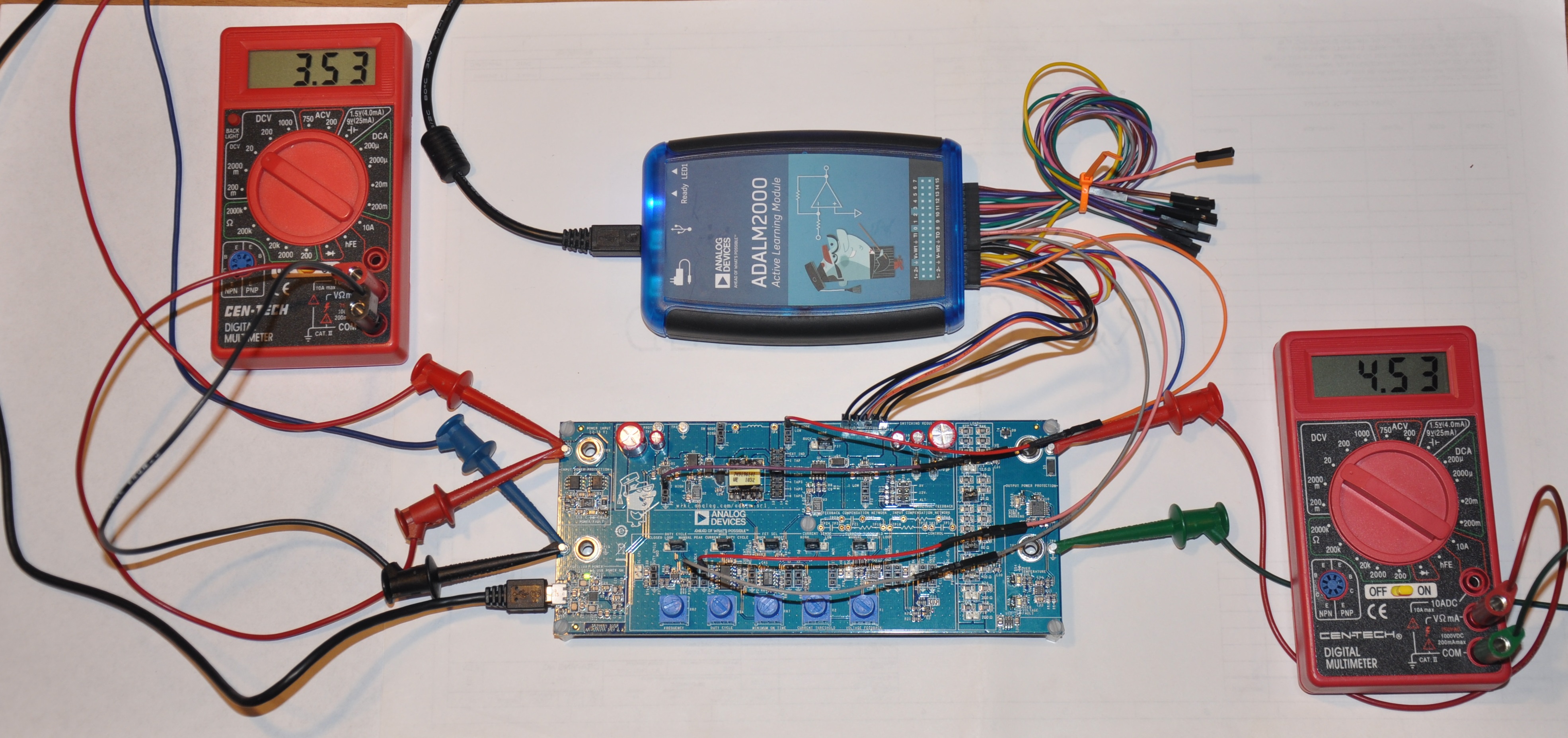
Figure 1a. ADSRALM Overview
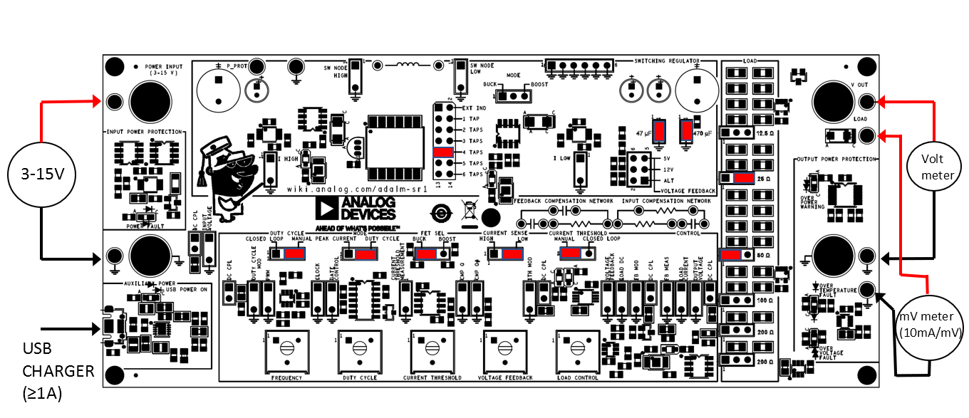
Figure 1b. ADSRALM Overview
ADALM-SR1 Jumpers and Connections
The ADALM-SR1 uses 0.635 mm (0.025-mil) headers for configuration jumpers, signal inputs, and signal outputs. Signal inputs and outputs are 2-conductor headers with 5.08 mm (200-mil) pitch so that they cannot be confused with configuration jumpers. The lower conductor is always a ground connection (that is not always used), and an arrow indicates whether the upper conductor is an input or output.

Figure 2. Topology, Mode Selection, and Loads
Inductance Selection
A Wurth 749196141 6-winding coupled inductor is used in both boost and buck configurations. The data sheet inductance for a single winding is 8.5 μH, with a DC resistance of 344 milliohms. The windings are connected in series on the ADALM-SR1, allowing the inductance to be changed, as noted in the table below. Values in the table are measured from a typical board.
| Inductance Selection (P3) | |||||||
|---|---|---|---|---|---|---|---|
| Jumper | |||||||
| Position | EXT IND | 1 TAP | 2 TAPS | 3 TAPS | 4 TAPS | 5 TAPS | 6 TAPS |
| Function | Ext. inductor at TP3, TP4 | 7.7μH inductance | 31.5μH inductance | 72.6μH inductance | 131.5μH inductance | 216.2μH inductance | 313.4μH inductance |
Output Capacitors Selection
A 4.7 μF capacitor is always connected to the output of the circuit. An additional 47 μF and 470 μF can be added by installing jumpers, as shown in the table below.
| Output Capacitors Selection | ||
|---|---|---|
| Jumper | P8, P11 | |
| Position | Installed | Open |
| Function | P8 connect additional 47μF capacitance | No additional capacitance |
| P11 connect additional 470μF capacitance | No additional capacitance | |
Load Resistors Selection
A resistive load may be connected to the output of the circuit. Resistances range from 12.5 Ω to 200 Ω and may be added in parallel, according to the table below. The jumpers are 3-position, with the right-hand position connecting the resistor to ground and the left-hand position allowing the effective resistance to be adjusted by Pulse-width-modulating the ground connection.
| Load Resistors Selection | ||
|---|---|---|
| Jumper | P18, P14, P13, P17, P16, P15 | |
| Position | Installed | Open |
| Function | P18 connect 200 Ω load resistance | No additional load resistor connected |
| P14 connect 200Ω load resistance | No additional load resistor connected | |
| P13 connect 100Ω load resistance | No additional load resistor connected | |
| P17 connect 50Ω load resistance | No additional load resistor connected | |
| P16 connect 25Ω load resistance | No additional load resistor connected | |
| P15 connect 12.5Ω load resistance | No additional load resistor connected | |
| Notes | 7 V max across 25Ω, 12.5Ω resistors will turn on the Over Power LED - which illuminates as a warning. | |
The R87 (LOAD CONTROL) potentiometer controls the duty cycle of all load resistors whose jumper is placed in the adjustable position by switching the ground connection. (YES this is super weird, but it's convenient, and works much better than you'd think!) Duty cycle is guaranteed to be zero when fully counter-clockwise and 100% when fully clockwise. Thus, the load can be a combination of fixed and variable resistances and the exact duty cycle of the onboard PWM circuit can be measured at P40. The signal at P40 has a 1k impedance and may be overdriven by a 3.3 V logic signal, allowing the load to be stepped.
The load PWM frequency is fixed at 200 kHz, approximately 10x the typical operating frequency of most experiments, thus appearing as a steady (DC) load.
A 0.1-ohm current sense resistor is in the ground return of the load resistors, allowing the total load current to be easily measured with the meter set to the 200 mV range at either the LOAD turret post (TP25) or the LOAD CURRENT jumper (P39).
Topology, FET, and Current Sense Selection
The selection between boost or buck topologies is made by jumpers P25, P35, and P37.
| FET Selection | Current Sense Selection | |||||
|---|---|---|---|---|---|---|
| Jumper | P37 | P35 | P25 | |||
| Position | BUCK | BOOST | BUCK | BOOST | HIGH | LOW |
| Function | Select buck topology | Select boost topology | Select the proper FET for buck topology | Select the proper FET for boost topology | Used for buck topology | Used for boost topology |
| Notes | Proper selection allows complete inductor waveform to be viewed. | |||||
In the boost configuration, P37 does not bypass Schottky diode D4; P35 routes the FET driver control to the low-side switch; and P25 selects the high-side current sense amplifier.
In the buck configuration, P37 bypasses D4; P35 routes the FET driver control to the high-side switch; and P24 selects the low-side current sense amplifier.
Close inspection of the operation of the circuit will show that, in theory, either current sense amplifier will work for both topologies. Still, the amplifier that is NOT at the switch node is chosen to minimize errors due to common-mode excursion.
Mode Selection
The ADALM-SR1 has several operational modes set by the jumpers, as noted below.
The MODE jumper selects between peak current mode and duty cycle control:
- Peak Current - a fixed frequency clock starts the inductor current ramp by turning on a MOSFET switch, and the switch opens when a peak current is reached.
- Duty Cycle - the duty cycle of the MOSFET switch is controlled directly.
| Control Mode Selection | ||
|---|---|---|
| Jumper | P32 | |
| Position | Peak Current | Duty Cycle |
| Function | Start on clock rising edge, stop on peak current | Direct duty cycle control |
| Notes | Closed/open-loop determined by Duty Cycle or Current Threshold jumper. | |
The peak current circuit is always active even in duty-cycle mode, increasing robustness in the event of an output short circuit.
Duty Cycle Source Selection
An LTC6992 Pulse-Width Modulator allows the switching MOSFET's duty cycle to be controlled directly, either manually by adjusting the DUTY CYCLE knob or under the control of the error amplifier.
| Duty Cycle Source Selection | ||
|---|---|---|
| Jumper | P23 | |
| Position | Closed-loop | Manual |
| Function | Duty controlled by error amplifier | Duty controlled by potentiometer |
| Notes | Current Threshold still operational for safety; determined by Current Threshold Potentiometer. | |
Current Threshold Source Selection
In peak-current control modes, the peak current can be controlled either manually by adjusting the CURRENT THRESHOLD knob or under the control of the error amplifier. The current threshold is also always active in voltage control modes, maintaining the per-cycle current limit as an added safety and robustness feature.
| Current Threshold Source Selection | ||
|---|---|---|
| Jumper | P22 | |
| Position | Manual | Closed-loop |
| Function | Threshold controlled by potentiometer | Threshold controlled by error amplifier |
| Notes | Set Duty Cycle pot to approx. 50%. (not critical, rising edge controls start of the ramp) | |
Feedback Selection
Three options for feedback network are provided, assuming a 1.25 V reference voltage. The 5V option is usually used for buck experiments (input voltage greater than 5 V), and the 12 V option is usually used for boost experiments (input less than 12 V). Footprints for optional 0603-sized resistors are included for user-defined feedback networks selected by the third jumper option.
| Feedback Selection | |||
|---|---|---|---|
| Jumper | P20 | ||
| Position | 5V | 12V | ALT |
| Function | Usually used for buck topology | Usually used for boost topology | Select user-installed feedback resistors |
Signal Measurement and Injection Points
The ADALM-SR1 provides numerous test points for stimulating (modulating) and measuring the operation of the circuit, such as input and output voltage, inductor current, and output current. Several aspects of the circuit's dynamic response can also be measured:
- In open-loop voltage mode, modulate the duty cycle control voltage to characterize the response of the power stage
- In open-loop current mode, modulate the current threshold (ITH) to characterize the response of the power stage
- In any closed-loop mode, modulate the feedback divider to characterize the closed-loop response of the whole circuit.
Connections are summarized in Figure X below and the following tables.

| Measurement Points | ||
|---|---|---|
| Name | Notes | |
| TP1 | P_PROT | Overvoltage/overcurrent protected power. |
| P1 | SW_NODE_HI | Switch node in buck topology. |
| P4 | SW_NODE_LOW | Switch node in boost topology. |
| P2 | IHIGH | Current sense amplifier output, boost configurations (0.1Ω sense R, G=7, 1.429 A/V net output). |
| P12 | ILOW | Current sense amplifier output, buck configurations (0.1Ω sense R, G=7, 1.429 A/V net output). |
| P10, P9, TP5, TP7 | V_OUT | Experiment output voltage. P10 can be AC coupled by removing P9. |
| P5 | FB_MEAS | Feedback perturbation measurement (AC coupled). |
| P33 | CLOCK | Master clock, 3.3V logic level. |
| P34 | GATE CONTROL | FET gate control signal, 3.3V logic level. |
| Injection Points | ||
|---|---|---|
| Name | Notes | |
| P28 | ITH MOD | Peak current control modulation (1.429 A/V). Install P29 to DC couple. |
| P27 | DUTY CYCLE MOD | Duty Cycle modulation (100%/V). Install P26 to DC couple. |
| P7 | FB_MOD | Feedback modulation for loop gain measurements (XXV/V). Install P6 to DC couple. |
Hardware Setup Procedure
Refer to individual lab exercises for detailed setup information.
Auxiliary Circuit Details
The setup and operation of circuitry associated with the lab exercises are described in detail in the exercises themselves. The ADALM-SR1 includes various auxiliary housekeeping and protection circuits described here.
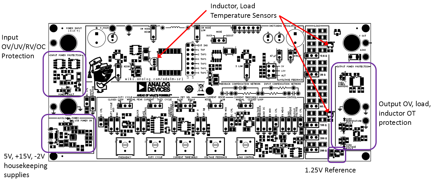
Housekeeping Supplies and Reference
The ADALM-SR1 has two power inputs. The user supplies the experiment power input, and the voltage will vary depending on the experiment being run. An additional micro USB connector is the input for a 5 V “housekeeping” supply that powers all of the control circuitry, allowing the experiment power to vary over a wide range. An LT3472 boosts or inverts the 5 V supply to +15 / -2 V, respectively. This provides a high voltage and slightly negative voltage for the LT1995 current sense amplifiers and a negative supply for the error amplifier.
An LT1970-1.25 provides an accurate reference for the error amplifier and duty cycle current threshold adjustment potentiometers.
Input Overvoltage, Undervoltage, Reverse voltage, and Overcurrent
The Figure below shows an LTspice schematic of the ADALM-SR1's protection circuitry. The simulation file is available at OL_engineer_proofing.asc, and running the simulation in LTspice will exercise some of the various fault conditions.

An LTC4368 and associated circuitry protects the experiment power input by only turning on when the supply is between 3 V and 15 V. The circuit is protected from voltages between -40 V and +60 V. The LTC4368 also functions as a fuse, shutting off the supply if the current exceeds 2 A.
Output Overvoltage
In boost mode, the ADSRALM can produce high voltages under certain conditions: if the duty cycle is high and the load is light, or if feedback is disconnected. An LTC2912 overvoltage / undervoltage supervisor will disable the switching circuitry if the output exceeds 22 V. An SMAJ24A, 24-volt TVS diode provides additional protection.
Inductor, Load Resistor Overtemperature
The inductor and onboard load resistors can get warm during certain experiments or if the board is misconfigured. Three temperature sensors measure the inductor temperature and the temperature of the high-dissipation areas of the load resistor bank. If any temperature exceeds 60ºC, switching is disabled for a 1.9 second cool-down period.
The low-resistance loads consist of parallel, single 100 Ω, 1/2 W resistors. An orange LED near the associated jumpers illuminates when the output voltage exceeds 7 V as a warning that these must be disconnected.
The high resistance loads consist of multiples of two 100-ohm, 1/4 W resistors in series, which will handle voltages up to 14 V. A temperature sensor is still included in case the output voltage exceeds 14 V or if the experiment is left running for an extended period of time.
Schematic, PCB Layout, Bill of Materials
ADALM-SR1 Design & Integration Files
- Schematics
- PCB Layout
- Bill of Materials
- Allegro Project
Corner Case Test Report
This is an informal internal test report intended to exercise operating conditions outside those detailed in the experiments. This may be useful for those developing additional exercises.
This page is for the released revision of the ADALM-SR1. Documentation for the pilot run (rev A) is here for reference: ADALM-SR1 hardware
End of Document
university/tools/lab_hw/adalm-sr1.txt · Last modified: 14 Mar 2023 06:38 by Joyce Velasco