


This version (04 Nov 2021 16:45) was approved by Mark Thoren.The Previously approved version (05 May 2021 23:38) is available.
Table of Contents
Activity: Boost Converters: closed loop operation
Objective:
Much of this exercise mirrors the Buck Converters: closed loop operation lab. The objective of this activity is to close the loop around the boost converter developed in the open-loop exercise such that the output voltage remains constant as the input voltage and output loading conditions vary. First, the loop will be closed in an “overcompensated” manner, such that the DC output voltage is correct, disregarding stability, transient response, and other AC parameters. The power stage AC response will then be characterized, essential in developing a robust and stable control loop. The loop will then be closed using the “obvious” method of voltage-mode control, that is, adjusting the duty cycle directly in response to an error in output voltage. Next, a current control loop will be introduced, and the advantages and disadvantages of this method explored.
The various LTspice analysis techniques are described in Buck Converters: closed loop operation, details are omitted in this activity.
Materials
- ADALM2000 (M2K) Active Learning module OR:
- Two-channel oscilloscope with external trigger input
- Two digital multimeters OR:
- additional ADALM2000
- ADALM-SR1 Switching Regulator Active Learning Module
- User Guide: ADALM-SR1 hardware
- EVAL-CN0508-RPIZ power supply OR:
- 0-12V, 3A Adjustable benchtop power supply
- LTspice files for this exercise
Background
A buck converter, while not necessarily a simple circuit, can be thought of of as an L-C-R filter, where a switching waveform is applied to the input of the filter, and the output is an averaged representation of the switching waveform. Boost converters, on the other hand, are a bit more mysterious - a low voltage is used to “charge” an inductor, storing energy in a magnetic field. This stored energy is then released into a load that is at a higher voltage than that used to charge the inductor… like magic.
Activity 1: An Overcompensated Voltage-Mode Boost Converter
Before we dig into too much theory, let's at least get the boost converter into regulation… The goal of this experiment is to produce an accurate output voltage, regardless of changes in input voltage (“line regulation”) and changes in output loading conditions (“load regulation”). We'll do this by dynamically changing the duty cycle of the PWM generator in response to changes in the output voltage - if the output voltage is a bit too high, reduce the PWM duty cycle. If the output voltage is a bit too low, increase the PWM duty cycle.
This is called “voltage mode” control because the error signal (how far we are off from the desired output voltage) directly controls the input voltage to output voltage ratio (set by the duty cycle.)
Figure 1 below shows the boost power stage from the open-loop exercise, but with the duty cycle potentiometer replaced by an op-amp circuit configured as an inverting integrator. This circuit compares a scaled version of the output voltage against an accurate 1.25V reference voltage, and performes the following actions, stated qualitiatively:
- If the output voltage is a little bit too low, the output voltage ramps up slowly.
- If the output voltage is MUCH too low, the output voltage ramps up quickly.
- If the output voltage is a little bit too high, the output voltage ramps down slowly.
- If the output voltage is MUCH too high, the output voltage ramps down quickly.
- And finally, if the output voltage is “just right”, hold the output voltage constant

Figure 1. Voltage Mode boost Converter
But since the integrator output is connected to the LTC6992-3's MOD pin, an increase / decrease in voltage will directly cause a corresponding increase / decrease in the MOSFET's duty cycle, which will tend to bring the output voltage toward the “just right” voltage.
Also note the following simplifications:
- LTC7001 gate driver replaced with a voltage-controlled voltage source with a gain of 1
- MOD positive clamp circuit replaced with an ideal diode and voltage source
Open the CL_boost_voltage_mode.asc simulaton, verify that the lower two 200Ω load resistors are connected (100Ω total load), and run it. Observe the turn-on transient, which has quite a bit of overshoot, but then stabilizes at 12.0V. Zoom in on the switch node and inductor current after the intial transient, shown in Figure 2. Note that the circuit is operating in DCM.

Figure 2. Voltage Mode boost Converter Simulation, switch node and inductor current
BEFORE APPLYING POWER… Configure the ADALM-SR1 board as shown in Figure 3 below:

Figure 3. ADALM-SR1 Configuration for Voltage Mode boost Operation
Install the following jumpers:
- VOLTAGE FEEDBACK: 12V
- Duty Cycle: CLOSED LOOP
- Mode: Duty Cycle
- FET Sel: BOOST
- Current Sense: HIGH
- Current Threshold: MANUAL
- Inductance: 4 Taps
- Load Resistors: enable 2×200Ω (100Ω total)
Set potentiometers to the following approximate settings:
- Frequency: 3:00
- Duty Cycle: 12:00
- Minimum On Time: 7:00 (fully counterclocwise)
- Current Threshold: 3:00
- Voltage Feedback: 5:00 (fully clockwise)
Additionally - install the following components:
- 0.1μF capacitor between TP22, TP24
- 10kΩ resistor between TP21, TP19
- 10kΩ resistor between TP14, TP17
Connect a 5V, 1A USB power supply to the Auxiliary Power micro USB jack. At this point, the frequency can be fine-tuned by looking at the D0 signal in Scopy's logic analyzer. Set the frequency to 20kHz (50μs period)
Ramp the Power Input to 5V and observe the current sense and switch node waveforms. Note that Scopy's vertical scale can be entered arbitrarily - enter a value of 280mV/Div, which corresponds to 400mA/Div. Figure 4 shows the measured results; compare with the simulated result in Figure 3.

Figure 4. Measured Results, switch node and inductor current
Decrease the load to 200Ω by removing one of the 200Ω jumpers and note that the duty cycle decreases automatically to maintain 12V at the output as shown in Figure 5.
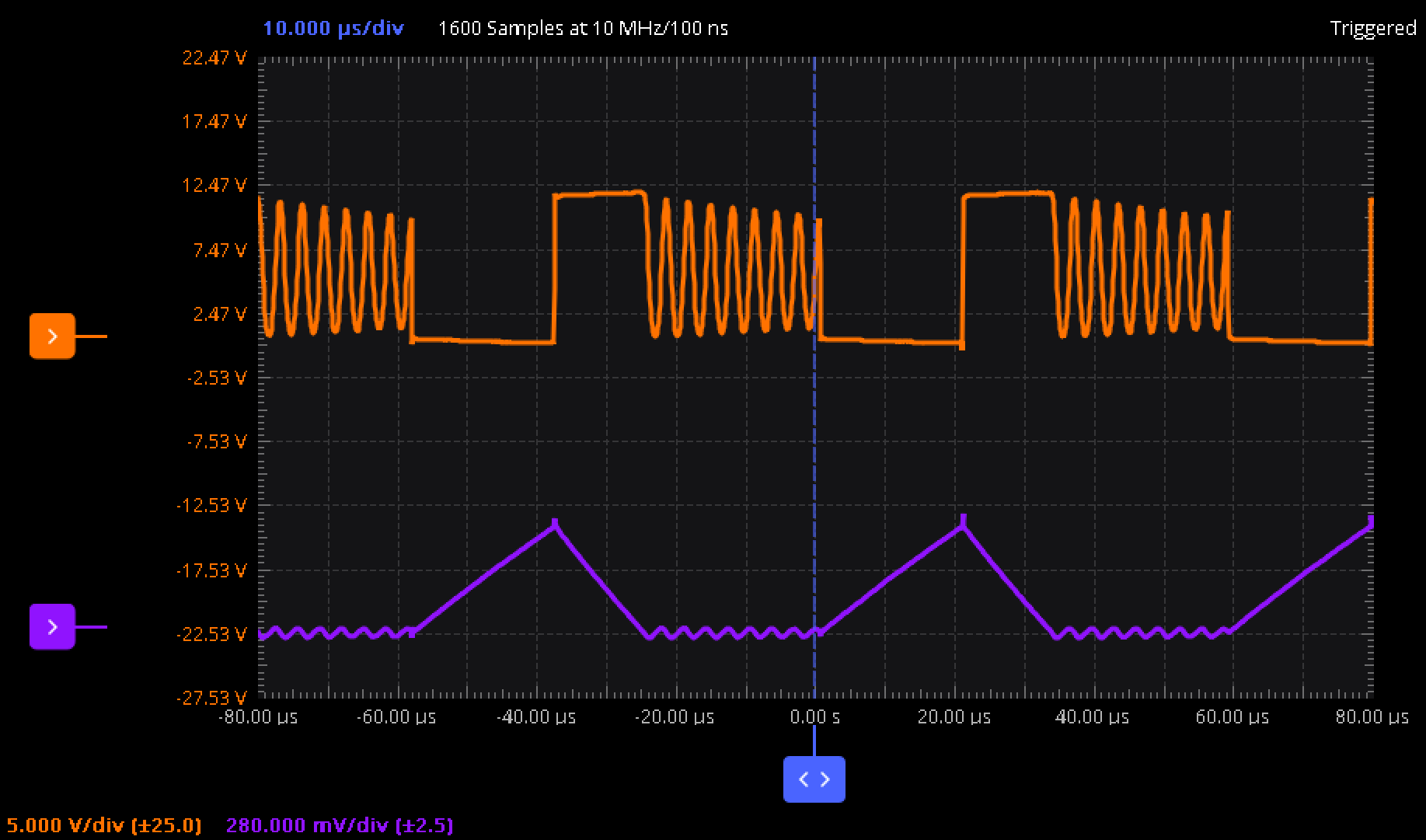
Figure 5. Measured switch node voltage and inductor current, 200Ω load
Adjusting the LTspice simulation accordingly shows close correlation to the measured results as shown in Figure 6.

Figure 6. Simulated switch node voltage and inductor current, 200Ω load
Activity 2: Closed-loop, current-mode, overcompensated for guaranteed stability
The goal of this experiment is identical to the previous one: to produce an accurate output voltage, regardless of changes in input voltage or output loading. But instead of directly changing the duty cycle of the PWM generator, we'll instead modulate the peak inductor current - if the output voltage is a bit too high, reduce the peak inductor current. If the output voltage is a bit too low, increase the peak inductor current.
This is called “current mode” control because of the error signal (how far we are off from the desired output voltage) is directly compared to the peak inductor controlling the current in the circuit. Conceptually this makes the inductor a controlled current source.
Consider Reordering, put after Voltage Mode is done.
Activity 3: Voltage-mode loop optimization
The previous examples were overcompensated so that the steady-state operation of the control loop could be analyzed, without too much concern that it would burst into oscillation. The next few experiments will demonstrate the drawback of overcompensation (slow response to changes in conditions), and outline the procedure for making it a bit more “snappy”, while still not oscillating.
The first step in speeding up the response by adjusting the compensator is to understand the response of the power stage to the output of the compensator. Or stated another way, to find the transfer function from a wiggle at the power stage's control input to the output actually moving. A great reference for some of these ideas is Linear Technology (Analog Devices) Application Note 47, Appendix C “The Oscillation Problem - Frequency Compensation Without Tears” (insert URL)
Boost Power Stage Continuous model, voltage-mode
Consider the ADALM-SR1 power stage when configured for open-loop, duty cycle control mode, with the LTC6992-3 PWM generator providing the gate control:
Dig into differences between boost and buck stages in terms of dynamic response, output impedance, etc.
Let's take our newfound knowledge of the power stage, and analyze the closed-loop response with the overcompensated compensator.
(predict linearized response, phase margin, then compare with ADALM-SR1 results)
(Measured results with ADALM-SR1 using Middlebrook circuit, step response and cutoff.)
(speed up compensator to some reasonable fraction of power stage, predict result, compare against ADALM-SR1)
Activity 4: Current-mode loop optimization
Intro on differences in control dynamics…
Return to Power Based Lab Activity Material
Return to Engineering University Program Home
university/labs/closed_loop_boost_adalm2000.txt · Last modified: 04 Nov 2021 16:45 by Mark Thoren