


This version is outdated by a newer approved version. This version (14 Aug 2017 08:31) was approved by erbe reyta.
This version (14 Aug 2017 08:31) was approved by erbe reyta.This is an old revision of the document!
Table of Contents
CN0273: High Speed FET Input Instrumentation Amplifier with Low Input Bias Current and High AC Common-Mode Rejection
OVERVIEW
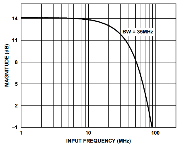
The circuit is a high speed FET input, gain-of-5 instrumentation amplifier (in-amp) with a wide bandwidth (35 MHz) and excellent ac common-mode rejection, CMR, (55 dB at 10 MHz). The circuit is ideal for applications where a high input impedance, fast in-amp is required, including RF, video, optical signal sensing, and high speed instrumentation. The high CMR and bandwidth also makes it ideal as a wideband differential line receiver. Ideal as a wideband differential line receiver.
DEMO REQUIREMENTS
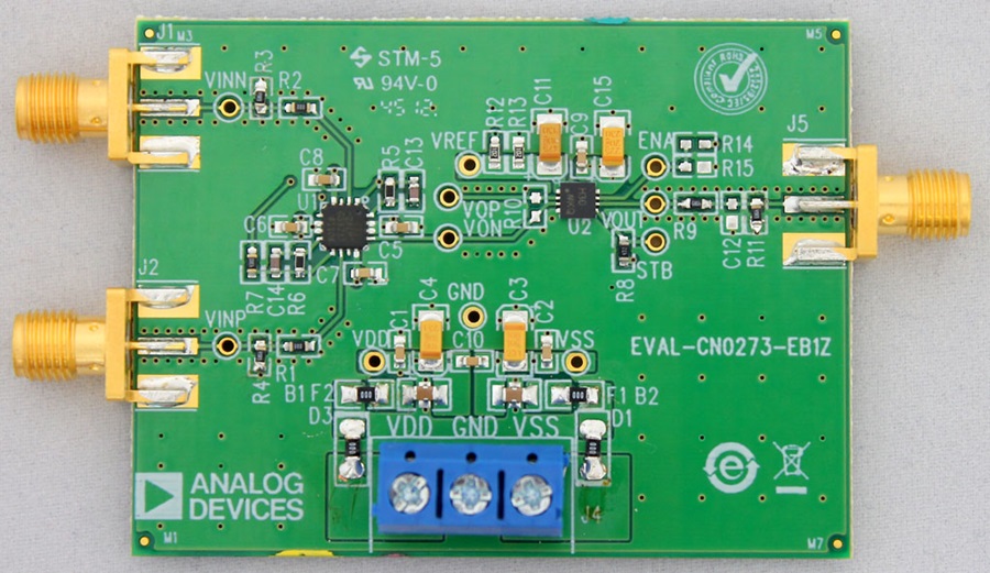
- EVAL-CN0273-EB1Z circuit evaluation board
- +/-5 V dual power supply
- Signal generator with a balanced differential drive source
- 3 SMA to BNC Connector
HARDWARE SETUP

Power Supply
+/-5V supply should be supplied to the connector for proper operation of the evaluation board
Input Signal
Signal Generator w/ Balanced Differential Drive Source can be used as an input source.
Peak to Peak Input Voltage Restriction
- Maximum allowable differential input is ±3.5 V/G1, where G1 is the gain of the first stage.
There is a tradeoff between the maximum allowable differential input and the closed-loop gain of the first stage.
Common Mode Input Voltage Restriction
- Allowable input common-mode range for the composite circuit is from −3.5 V to +2.2 V
Bandwidth Input Restriction
- Allowable input frequency bandwidth is 35MHz @ -3dB, typical for G = 5
Output Measurement
Oscilloscope can be used to measure the output of the evaluation board with a gain of 14db below 10Mhz input as indicited in the graph below.
The output swing of the circuit is limited to ±3.5 V when operating on ±5 V supplies
ADVANCED CONFIGURATION

FET Amplifier Input Gain Stage
- The circuit has a differential inputs gain of 1 + 2RF/RG
- Where,
- RF = Resistor R5 and R6
- RG = Resistor R7
- For this circuit, a feedback resistor of 200 Ω was chosen. The feedback capacitor, CF, was 2 pF for the best bandwidth flatness.
- When the inputs are common-mode, there is no current flowing through the RG gain resistor. Thus, the circuit acts as a buffer for the common-mode inputs.
SCHEMATICS, PCB LAYOUT, BILL OF MATERIALS
- Schematics (PDF)
- Bill of Materials (Excel)
- Layout Gerbers (ZIP)
- Assembly Drawing (PDF)
End of Document
resources/eval/user-guides/circuits-from-the-lab/cn0273.1502692245.txt.gz · Last modified: 14 Aug 2017 08:30 by erbe reyta