


This version (29 Jul 2021 06:05) was approved by Harvey John De Chavez.The Previously approved version (03 Jan 2021 21:55) is available.
Table of Contents
CN0273: High Speed FET Input Instrumentation Amplifier with Low Input Bias Current and High AC Common-Mode Rejection
OVERVIEW
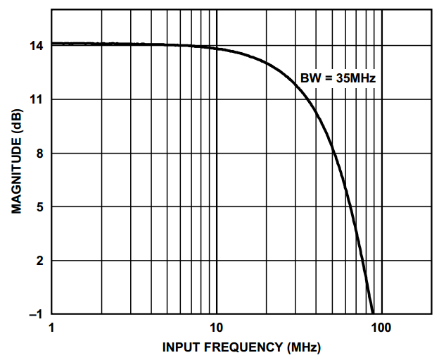
The circuit is a high speed FET input, gain-of-5 instrumentation amplifier (in-amp) with a wide bandwidth (35 MHz) and excellent ac common-mode rejection, CMR, (55 dB at 10 MHz). The circuit is ideal for applications where a high input impedance, fast in-amp is required, including RF, video, optical signal sensing, and high speed instrumentation. The high CMR and bandwidth also makes it ideal as a wideband differential line receiver. Ideal as a wideband differential line receiver.
DEMO REQUIREMENTS
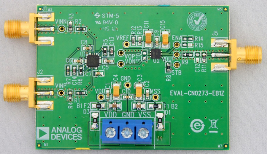
- EVAL-CN0273-EB1Z circuit evaluation board
- +/-5 V dual power supply
- Signal generator with a balanced differential drive source
- 3 SMA to BNC Connector
HARDWARE SETUP

Power Supply
+/-5V supply should be supplied to the connector for proper operation of the evaluation board
Input Signal
Signal Generator w/ Balanced Differential Drive Source can be used as an input source.
Peak to Peak Input Voltage Restriction
- Maximum allowable differential input is ±3.5 V/G1, where G1 is the gain of the first stage.
There is a tradeoff between the maximum allowable differential input and the closed-loop gain of the first stage.
Common Mode Input Voltage Restriction
- Allowable input common-mode range for the composite circuit is from −3.5 V to +2.2 V
Bandwidth Input Restriction
- Allowable input frequency bandwidth is 35MHz @ -3dB, typical for G = 5
Output Measurement
Oscilloscope can be used to measure the output of the evaluation board with a gain of 14db below 10Mhz input as indicited in the graph below.
The output swing of the circuit is limited to ±3.5 V when operating on ±5 V supplies
ADVANCED CONFIGURATION

FET Amplifier Input Gain Stage
- The circuit has a differential inputs gain of 1 + 2RF/RG
- Where,
- RF = Resistor R5 and R6
- RG = Resistor R7
- For this circuit, a feedback resistor of 200 Ω was chosen. The feedback capacitor, CF, was 2 pF for the best bandwidth flatness.
- When the inputs are common-mode, there is no current flowing through the RG gain resistor. Thus, the circuit acts as a buffer for the common-mode inputs.
SCHEMATICS, PCB LAYOUT, BILL OF MATERIALS
- Schematics (PDF)
- Bill of Materials (Excel)
- Layout Gerbers (ZIP)
- Assembly Drawing (PDF)
Registration
Receive software update notifications, documentation updates, view the latest videos, and more when you register your hardware. Register to receive all these great benefits and more!
End of Document
resources/eval/user-guides/circuits-from-the-lab/cn0273.txt · Last modified: 29 Jul 2021 06:05 by Harvey John De Chavez