


This version is outdated by a newer approved version. This version (25 Nov 2021 08:30) was approved by Laszlo Nagy.The Previously approved version (29 Jul 2021 12:50) is available.
This version (25 Nov 2021 08:30) was approved by Laszlo Nagy.The Previously approved version (29 Jul 2021 12:50) is available.This is an old revision of the document!
Table of Contents
AXI_ADRV9001/AXI_ADRV9002 Interface Core
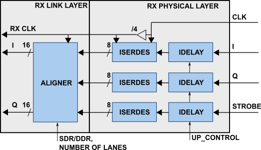
Block diagram

Parameters
| Parameter name | Default value | Description |
|---|---|---|
| CMOS_LVDS_N | 0 | Source synchronous interface type; 0 - LVDS ; 1 - CMOS |
| TDD_DISABLE | 0 | Controls the insertion of the TDD core. If set the TDD controller won't be part of the implementation. |
| DDS_DISABLE | 0 | If resource utilization is a concern, by setting this parameter you can remove the dual tone DDS logic from the Tx channels. This will reduce resource utilization significantly but loosing the ability to generate a test tone. |
| INDEPENDENT_1R1T_SUPPORT | 1 | 0 - Rx2 (adc_2_*) and Tx2 (dac_2_*) data channels will be disabled; RX2 TPL, TX2 TPL cores are disabled. 1 - Allows independent control of Rx2/Tx2 PHY either from Rx12/Tx12 TPL or Rx2/Tx2 TPL blocks; |
| COMMON_2R2T_SUPPORT | 1 | 0 - puts the Rx12/Tx12 TPL in R1_MODE, having access only to Rx1/Tx1 PHYs; 1 - Allows Rx12/Tx12 TPL to operate in 2R 2T mode having control over Rx2/Tx2 PHY |
| RX_USE_BUFG | 0 | Used in case of Xilinx 7 series devices; If set, will insert a global clock buffer on the Rx clock path. Useful if user logic does not fits in a clock region. |
| TX_USE_BUFG | 0 | Used in case of Xilinx 7 series devices; If set, will insert a global clock buffer on the Tx clock path. Useful if user logic does not fits in a clock region. |
| USE_RX_CLK_FOR_TX | 0 | In case the received clock on the Tx source synchronous interface is not routed to clock capable pins, when setting this to 1 the Rx clock will be used to drive the Tx interface |
| IO_DELAY_GROUP | “dev_if_delay_group” | Used in case of Xilinx devices. Identifier of the IODELAYCTRL cell. |
| FPGA_TECHNOLOGY | 0 | Auto populated by IPI. |
| FPGA_FAMILY | 0 | Auto populated by IPI. |
| SPEED_GRADE | 0 | Auto populated by IPI. |
| DEV_PACKAGE | 0 | Auto populated by IPI. |
Register Map
The register map of the core contains instances of several generic register maps like ADC common, ADC channel, DAC common, DAC channel etc. The following table presents the base addresses of each instance, after that can be found the detailed description of each generic register map. The absolute address of a register should be calculated by adding the instance base address to the registers relative address.
Register Map base addresses for axi_ad9001
| Address | Name | Description | |||
| DWORD | BYTE | ||||
| 0x0000 | 0x0000 | RX1 BASE | See the Base (common to all cores) table for more detail | ||
|---|---|---|---|---|---|
| 0x0000 | 0x0000 | RX1 COMMON | See the ADC Common table for more detail | ||
| 0x0000 | 0x0000 | RX1 CHANNELS | See the ADC Channel table for more detail | ||
| 0x0200 | 0x0800 | RX1 Delay control | See the IO Delay Control table for more detail | ||
| 0x0400 | 0x1000 | RX2 BASE | See the Base (common to all cores) table for more detail | ||
| 0x0400 | 0x1000 | RX2 COMMON | See the ADC Common table for more detail | ||
| 0x0400 | 0x1000 | RX2 CHANNELS | See the ADC Channel table for more detail | ||
| 0x0600 | 0x1800 | RX2 Delay control | See the IO Delay Control table for more detail | ||
| 0x0800 | 0x2000 | TX1 BASE | See the Base (common to all cores) table for more detail | ||
| 0x0800 | 0x2000 | TX1 COMMON | See the DAC Common table for more detail | ||
| 0x0800 | 0x2000 | TX1 CHANNELS | See the DAC Channel table for more detail | ||
| 0x1000 | 0x4000 | TX2 BASE | See the Base (common to all cores) table for more detail | ||
| 0x1000 | 0x4000 | TX2 COMMON | See the DAC Common table for more detail | ||
| 0x1000 | 0x4000 | TX2 CHANNELS | See the DAC Channel table for more detail | ||
| 0x1200 | 0x4800 | TDD1 | See the Transceiver TDD Control table for more detail | ||
| 0x1300 | 0x4C00 | TDD2 | See the Transceiver TDD Control table for more detail | ||
Base (common to all cores)
ADC Common (axi_ad*)
ADC Channel (axi_ad*)
DAC Common (axi_ad)
DAC Channel (axi_ad*)
IO Delay Control (axi_ad*)
Transceiver TDD Control (axi_ad*)
Physical Interface
The following operation modes are supported by the physical layer. CMOS (CSSI) and LVDS (LSSI) selection is done through synthesis parameter. Other parameter (column B, G, H) can be run time modified preferably while the core is in reset.
| A | B | C | D | E | F | G | H |
|---|---|---|---|---|---|---|---|
| CSSI 1-lane | 1 | 32 | 80 | 80 | 2.5 | SDR | 8 |
| CSSI 1-lane | 1 | 32 | 160 | 80 | 5 | DDR | 4 |
| CSSI 1-lane* | 1 | 16 | 80 | 80 | - | SDR | 4 |
| CSSI 1-lane* | 1 | 16 | 160 | 80 | - | DDR | 2 |
| CSSI 1-lane** | 1 | 8 | 80 | 80 | - | SDR | 2 |
| CSSI 1-lane** | 1 | 8 | 160 | 80 | - | DDR | 1 |
| CSSI 4-lane | 4 | 8 | 80 | 80 | 10 | SDR | 2 |
| CSSI 4-lane | 4 | 8 | 160 | 80 | 20 | DDR | 1 |
| LSSI 1-lane | 1 | 32 | 983.04 | 491.52 | 30.72 | DDR | 4 |
| LSSI 2-lane | 2 | 16 | 983.04 | 491.52 | 61.44 | DDR | 2 |
* ADRV9001 data port transmit/receive 16-bit data symbols
** ADRV9001 data port transmit/receive 8-bit data symbols. In case of 8-bit and 2-bit data symbols we'll use aligned MSBs
Columns description:
- A - SSI Modes
- B - Data Lanes Per Channel
- C - Serialization factor Per data lane
- D - Max data lane rate(MHz)
- E - Max Clock rate (MHz)
- F - Max Sample Rate for I/Q (MHz)
- G - Data Type
- H - User Interface Clock to Sample Clock ratio (aka DDS Rate) for Xilinx devices
The following equations apply:
where :
- number of bits transferred in a second per active lane
- represents the source synchronous interface clock frequency
- represents the frequency of the clock the user interface logic is connected
- represents the division factor the source synchronous interface clock is divided to get the user interface clock. This is implementation specific. Xilinx CMOS and LVDS = 4; Intel CMOS = 1
Since the is an integer multiple (column H) of the
the interface toward the user logic has a valid qualifier which is not active on every clock cycle.
Configure DAC common interface
Register 0x0048 REG_CNTRL_2
- [12:8] - NUM_LANES (new) - number of active lanes (1 : CSSI 1-lane, LSSI 1-lane, 2 : LSSI 2-lane, 4 : CSSI 4-lane)
- [14] - SYMB_8_16B (new) - select number of bits for symbol format mode (1 represents 8b, 0 represents 16b)
- [15] - SYMB_OP (new) - select symbol data format mode
- [16] - SDR_DDR_N (new) - interface type (1 represents SDR, 0 represents DDR)
Register 0x04c REG_RATECNTRL
- [7:0] RATE - must be set according to column H of the table
Configure ADC common interface
Register 0x0044 REG_CNTRL
- [12:8] - NUM_LANES (new) - number of active lanes (1 : CSSI 1-lane, LSSI 1-lane, 2 : LSSI 2-lane, 4 : CSSI 4-lane)
- [14] - SYMB_8_16B (new) - select number of bits for symbol format mode (1 represents 8b, 0 represents 16b)
- [15] - SYMB_OP (new) - select symbol data format mode
- [16] - SDR_DDR_N (new) - interface type ( 1 represents SDR, 0 represents DDR)
Requirements
- Rx1 clock and Rx2 clock should be length matched
- Clock and data in SSI interface must be length matched
Xilinx Physical interface
RX Component mode
For Rx interfaces the source synchronous associated clock is used to sample the input data. Software configuration is required described in Configure ADC common interface section. Input delays of the FPGA or output delays of the ADRV9001 can be tuned by software for optimize sampling.
TX Using dedicated clock
For Tx interfaces the clock received from the transceiver is used to drive the output data. Software configuration is required for clock rate selection described in Configure DAC common interface section. Input delays of the ADRV9001 can be tuned by software for optimize sampling.

More Information
Support
Analog Devices will provide limited online support for anyone using the reference design with Analog Devices components via the EngineerZone.
resources/eval/user-guides/adrv9002/axi_adrv9002.1637749874.txt.gz · Last modified: 24 Nov 2021 11:31 by Laszlo Nagy