System architecture
ADI Reference Design System Architecture
Every HDL design of a reference project can be divided into two subsystems:
The base design containing an embedded processor - soft or hard - and all the peripheral IPs that the carrier board supports and are necessary to run a Linux distribution on the system. These designs are carrier dependent, each prototyping board having its own base design.
The board design is a direct integration of all the necessary IP used to support an FMC I/O board. These designs are carrier independent and common to all carrier boards.

DAQ2 Hardware Architecture


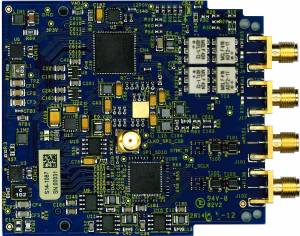
The AD-FMCDAQ2-EBZ module is comprised of the AD9680 dual, 14-bit, 1.0 GSPS, JESD204B ADC, the AD9144 quad, 16-bit, 2.8 GSPS, JESD204B DAC, the AD9523-1 clock, and power management components.
A functional block diagram of the system is given below. The system consists of four functional partitions - transmit path, receive path, clocking, control interfaces and power management.
Transmit Path
The reference design generates the signals for AD9144, using the JESD204B interface to transfer data and SPI and GPIO for controlling the part. The JESD204B connection is done through 4 lanes at 10Gbps.
Receive Path
The reference design captures data from the AD9680 through the JESD204B interface and uses SPI and GPIO for controlling the part. The JESD204B connection is done through 4 lanes at 10Gbps.
Clocking
The system is clocked through an on board crystal (125MHz). The clock path mainly consists of the AD9523-1 which upconverts this signal to ~3GHz, and then divides this back down to any integer divider of this ~3GHz output.
The default reference design that ADI provides does the following:
Crystal generates a fixed clock frequency of 125MHz.
This clock is sent to the AD9523-1.
An internal VCO clock of between 2940
MHz to 3100
MHz. Since it includes an integer-based feedback divider, it only allows integer frequency multiplication (multiples of 125
MHz), the only multiplier that works in that range is 24, to give us a VCO rate of 3000
MHz.
This VCO output must go through a divider of or 3, 4, or 5, providing a max output clock of 1000
MHz This 1000
MHz is then divided down to provide:
1000
MHz for the DAC sample rate
1000
MHz for the ADC sample rate
500
MHz for the reference clocks to FPGA
These rates can be changed, but only based on the limitations of the AD9523-1, the lowest JESD clocks the FPGA will support, and the min number of lanes the ADC and DAC support. The JESD Interface framework understands all these heuristics, and configures everything accordingly.
The AD9523-1 also supplies the SYSREF signal to all parts of the JESD204B system allowing for deterministic latency in the system.
References