


This version (23 Jan 2024 10:37) was approved by Adrian Costina.The Previously approved version (08 Jun 2022 15:52) is available.
Table of Contents
JESD204B/C Link Transmit Peripheral
The Analog Devices JESD204B/C Link Transmit Peripheral implements the link layer handling of a JESD204 transmit logic device. Implements the 8B/10B based link layer defined in JESD204C standard that is similar to the link layer defined in JESD204B. This includes handling of the SYSREF and SYNC~ and controlling the link state machine accordingly as well as performing per lane scrambling and character replacement. It has been designed for interoperability with Analog Devices JESD204B DAC converter products. Implements the 64B/66B based link layer defined in the JESD204C standard. This includes handling of the SYSREF, per lane encoding of sync header, scrambling as per data multi-block CRC generation.
The type of link layer is selectable during implementation phase through the LINK_MODE synthesis parameter.
To form a complete JESD204 transmit logic device it has to be combined with a PHY layer and transport layer peripheral.
Features
- Backwards compatibility with JESD202B
- 64B/66B link layer defined in JESD204C
- Subclass 0 and Subclass 1 support
- Deterministic Latency (for Subclass 1 operation)
- Runtime re-configurability through memory-mapped register interface (AXI4)
- Interrupts for event notification
- Diagnostics
- Max Lanerate with 8B/10B mode: 15 Gbps
- Max Lanerate with 64B/66B mode: 32 Gbps
- Low Latency
- Independent per lane enable/disable
Utilization
Files
| Name | Description |
|---|---|
| axi_jesd204_tx.v | Verilog source for the peripheral. |
| axi_jesd204_tx_ip.tcl | TCL script to generate the Vivado IP-integrator project for the peripheral. |
Block Diagram

Synthesis Configuration Parameters
| Name | Description | Default |
|---|---|---|
ID | Instance identification number. | 0 |
NUM_LANES | Maximum number of lanes supported by the peripheral. | 1 |
NUM_LINKS | Maximum number of links supported by the peripheral. | 1 |
LINK_MODE | Decoder selection of the link layer. 1 - 8B/10B mode 2 - 64B/66B mode | 1 |
DATA_PATH_WIDTH | Data path width in bytes. Set it 4 in case of 8B/10B, 8 in case of 64B/66B | 4 |
TPL_DATA_PATH_WIDTH | Data path width in bytes towards transport layer. Must be greater or equal to DATA_PATH_WIDTH. Must be a power of 2 integer multiple of the F parameter. | 4 |
ASYNC_CLK | Set this parameter to 1 if the link clock and the device clocks have different frequencies, or if they have the same frequency but a different source. If set, synchronizing logic and a gearbox of ratio DATA_PATH_WIDTH:TPL_DATA_PATH_WIDTH is inserted to do the rate conversion. If not set, TPL_DATA_PATH_WIDTH must match DATA_PATH_WIDTH, the same clock must be connected to clk and device_clk inputs. | 0 |
Signal and Interface Pins
| Name | Type | Description |
|---|---|---|
s_axi_aclk | Clock | All S_AXI signals and irq are synchronous to this clock. |
s_axi_aresetn | Synchronous active low reset | Resets the internal state of the peripheral. |
S_AXI | AXI4-Lite bus slave | Memory mapped AXI-lite bus that provides access to modules register map. |
irq | Level-High Interrupt | Interrupt output of the module. Is asserted when at least one of the modules interrupt is pending and enabled. |
clk | Clock | Link clock for the JESD204 interface. Must be line clock / 40 for correct operation in 8B/10B mode, line clock / 66 in 64B/66B mode. |
reset | Reset | Reset active high synchronous with the Link clock. |
device_clk | Clock | Device clock for the JESD204 interface. Its frequency must be link clock * DATA_PATH_WIDTH / TPL_DATA_PATH_WIDTH |
device_reset | Reset | Reset active high synchronous with the Device clock. |
TX_DATA | AXI4-Streaming interface | Transmit data. |
sync[m-1:0] | Input | The m-th JESD204B SYNC~ (or SYNC_N) signal, available in 8B/10B mode. (0 <= n < NUM_LINKS) |
sysref | Input | JESD204 SYSREF signal. |
TX_PHYn | JESD204 transmit PHY interface | n-th lane of the JESD204 interface (0 <= n < NUM_LANES). |
Register Map
JESD204 TX (axi_jesd204_tx)
| Access Type | Name | Description |
|---|---|---|
| RO | Read-only | Reads will return the current register value. Writes have no effect. |
| RW | Read-write | Reads will return the current register value. Writes will change the current register value. |
| RW1C | Write-1-to-clear | Reads will return the current register value. Writing the register will clear those bits of the register which were set to 1 in the value written. |
| V | Volatile | The V suffix indicates that the register is volatile and its content might change without software interaction. The value of registers without the volatile designation will change without an explicit write done by software. |
Theory of Operation
The JESD204B/C transmit peripheral consists of two main components. The register map and the link processor. Both components are fully asynchronous and are clocked by independent clocks. The register map is in the s_axi_aclk clock domain, while the link processor is in the clk and device_clk clock domain.
The register map is used to configure the operational parameters of the link processor as well as to query the current state of the link processor. The link processor itself is responsible for handling the JESD204 link layer protocol.
Interfaces and Signals
Register Map Configuration Interface
The register map configuration interface can be accessed through the AXI4-Lite S_AXI interface. The interface is synchronous to the s_axi_aclk. The s_axi_aresetn signal is used to reset the peripheral and should be asserted during system startup until the s_axi_aclk is active and stable. De-assertion of the reset signal should by synchronous to s_axi_aclk.
JESD204B Control Signals
The sync and sysref signals corresponds to the SYNC~ and SYSREF signals of the JESD204 specification. These are signals generated externally and need to be connected to the peripheral for correct operation.
In 8B/10B link layer the sysref signal is optional and only required to achieve deterministic latency in subclass 1 mode operation. If the sysref signal is not connected software needs to configure the peripheral accordingly to indicate this. In 64B/66B link layer the sysref signal is mandatory.
When the sysref signal is used, in order to ensure correct operation, it is important that setup and hold of the external signal relative to the device_clk signal are met. Otherwise deterministic latency can not be guaranteed.
Transceiver Interface (TX_PHYn)
For each lane the peripheral has one corresponding TX_PHY interface. These interfaces provide the pre-processed physical layer data. The TX_PHY interfaces should be connected to the down-stream physical layer transceiver peripheral.
The physical layer peripheral receiving data from these interfaces are responsible for performing the final 8b10b mapping as well as serializing the data and transmitting it on the physical CML differential high-speed serial lane.
User Data Interface (TX_DATA)
User data is accepted on the the AXI4-Stream TX_DATA interface. The interface is a reduced AXI4-Stream interface and only features the TREADY flow control signal, but not the TVALID flow control signal. The behavior of the interface is as if the TVALID signal was always asserted. This means as soon as tx_ready is asserted a continuous stream of user data must be provided on tx_data.

After reset and during link initialization the tx_ready signal is de-asserted. As soon as the User Data Phase is entered the tx_ready will be asserted to indicate that the peripheral is now accepting and processing the data from the tx_data signal. The tx_ready signal stays asserted until the link is either deactivated or re-initialized.

Typically the TX_DATA interface is connected to a JESD204B transport layer peripheral that provides framed and lane mapped data. The internal data path width of the peripheral is four, this means that four octets per lane are processed in parallel. When in the user data phase the peripheral expects to receive data for four octets for each lane in each beat.
This means that TX_DATA interface is DATA_PATH_WIDTH * 8 * NUM_LANES bits wide. With each block of consecutive DATA_PATH_WIDTH * 8 bits corresponding to one lane. The lowest DATA_PATH_WIDTH * 8 bits correspond to the first lane, while the highest DATA_PATH_WIDTH * 8 bits correspond to the last lane.
E.g. for 8B/10B mode where DATA_PATH_WIDTH=4. Each lane specific 32 bit block corresponds to four octets each 8 bits wide. The temporal ordering of the octets is from LSB to MSB, this means the octet placed in the lowest 8 bits is transmitted first, the octet placed in the highest 8 bits is transmitted last.
Data corresponding to lanes that have been disabled are ignored and their value is don't care.
Configuration Interface
The peripheral features a register map configuration interface that can be accessed through the AXI4-Lite S_AXI port. The register map can be used to configure the peripherals operational parameters, query the current status of the device and query the features supported by the device.
Peripheral Identification and HDL Synthesis Settings
The peripheral contains multiple registers that allow the identification of the peripheral as well as the discovery of features that were configured at HDL synthesis time. Apart from the SCRATCH register all registers in this section are read-only and write to them will be ignored.
The VERSION (0x000) register contains the version of the peripheral. The version determines the register map layout and general features supported by the peripheral. The version number follows semantic versioning. Increments in the major number indicate backward incompatible changes, increments in the minor number indicate backward compatible changes, patch letter increments indicate a bug fix.
The PERIPHERAL_ID (0x004) register contains the value of the ID HDL configuration parameter that was set during synthesis. Its primary function is to allow to distinguish between multiple instances of the peripheral in the same design.
The SCRATCH (0x008) register is a general purpose 32-bit register that can be set to an arbitrary values. Reading the register will yield the value previously written (The value will be cleared when the peripheral is reset). Its content does not affect the operation of the peripheral. It can be used by software to test whether the register map is accessible or store custom peripheral associated data.
The IDENTIFICATION (0x00c) register contains the value of “204T”. This value is unique to this type of peripheral and can be used to ensure that the peripheral exists at the expected location in the memory mapped IO register space.
The SYNTH_NUM_LANES (0x010) register contains the value of the NUM_LANES HDL configuration parameter that was set during synthesis. It corresponds to the maximum of lanes supported by the peripheral. Possible values are between 1 and 32.
The SYNTH_DATA_PATH_WIDTH (0x014) register contains the value of the internal data path width per lane in octets. This is how many octets are processed in parallel on each lane and affects the restrictions of possible values for certain runtime configuration registers. The value is encoded as the log2() of the data path width. Possible values are:
- 1: Internal data path width is 2
- 2: Internal data path width is 4
- 3: Internal data path width is 8
Interrupt Handling
Interrupt processing is handled by three closely related registers. All three registers follow the same layout, each bit in the register corresponds to one particular interrupt.
When an interrupt event occurs it is recorded in the IRQ_SOURCE (0x088) register. For a recorded interrupt event the corresponding bit is set to 1. If an interrupt event occurs while the bit is already set to 1 it will stay set to 1.
The IRQ_ENABLE (0x080) register controls how recorded interrupt events propagate. An interrupt is considered to be enabled if the corresponding bit in the IRQ_ENABLE register is set to 1, it is considered to be disabled if the bit is set to 0.
Disabling an interrupt will not prevent it from being recorded, but only its propagation. This means if an interrupt event was previously recorded while the interrupt was disabled and the interrupt is being enabled the interrupt event will then propagate.
An interrupt event that has been recorded and is enabled propagates to the IRQ_PENDING (0x084) register. The corresponding bit for such an interrupt will read as 1. Disabled or interrupts for which no events have been recorded will read as 0. Also if at least one interrupt has been recorded and is enabled the external irq signal will be asserted to signal the IRQ event to the upstream IRQ controller.
A recorded interrupt event can be cleared (or acknowledged) by writing a 1 to the corresponding bit to either the IRQ_SOURCE or IRQ_PENDING register. It is possible to clear multiple interrupt events at the same time by setting multiple bits in a single write operation.
For more details regarding interrupt operation see the interrupts section of this document.
Link Control
The LINK_DISABLE (0x0c0) register is used to control the link state and switch between enabled and disabled. While the link is disabled its state machine will remain in reset and it will not react to any external event like the SYSREF or SYNC~ signals.
Writing a 0 to the LINK_DISABLE register will enable the link. While the link state is changing from disabled to enabled it will go through a short initialization procedure, which will take a few clock cycles. To check whether the initialization procedure has completed and the link is fully operational the LINK_STATE (0x0c4) register can be checked. This register will contain a 0 when the link is fully enabled and will contain a 1 while it is disabled or going through the initialization procedure.
Writing a 1 to the LINK_DISABLE register will immediately disable the link.
The EXTERNAL_RESET ([1]) bit in the LINK_STATE register indicates whether the external link reset signal is asserted (1) or de-asserted (0). When the external link reset is asserted the link is disabled regardless of the setting of LINK_DISABLE. The external link reset is controlled by the fabric and might be asserted if the link clock is not stable yet.
Multi-link Control
A multi-link is a link where multiple converter devices are connected to a single logic device (FPGA). All links involved in a multi-link are synchronous and established at the same time. For an 8B/10B TX link, this means that the FPGA receives multiple SYNC signals, one for each link.
For a 8B/10B link the MULTI_LINK_DISABLE register allows activating or deactivating each SYNC~ lines independently. This is useful when depending on the use case profile some converter devices are supposed to be disabled.
Link Configuration
The link configuration registers control certain aspects of the runtime behavior of the peripheral. Since the JESD204 standard does now allow changes to link configuration while the link is active the link configuration registers can only be modified while the link is disabled. As soon as it is enabled the configuration registers turn read-only and any writes to them will be ignored.
The LANES_DISABLE (0x200) register allows to disable individual lanes. Each bit in the register corresponds to a particular lane and indicates whether that lane is enabled or disabled. Bit 0 corresponds to the first lane, bit 1 to the second lane and so on. A value of 0 for a specific bit means the corresponding lane is enabled, a value of 1 means the lane is disabled. A disabled lane will not transmit any data when the link is otherwise active. By default, all lanes are enabled.
The LINK_CONF0 register configures the octets-per-frame and frames-per-multi-frame settings of the link. The OCTETS_PER_FRAME ([18:16]) field should be set to the number of octets-per-frame minus 1 (F - 1). The OCTETS_PER_MULTIFRAME ([9:0]) field should be set to the number of octets-per-frame multiplied by the number of frames-per-multi-frame minus 1 (FxK - 1). For correct operation FxK must be a multiple of DATA_PATH_WIDTH. In 64B/66B mode this field matches and also represents the number of octets per extended multiblock (Ex32x8 - 1).
The LINK_CONF1 register controls the optional link level processing stages. The SCRAMBLER_DISABLE ([0]) bit controls whether scrambling of the transmitted user data is enabled or disabled. A value of 0 enables scrambling and a value of 1 disables it. In 64B/66B mode scrambling must be always enabled. The CHAR_REPLACEMENT_DISABLE ([1]) bit controls whether alignment character replacement is performed or not. A value of 0 enables character replacement and a value of 1 disables it.
Both the transmitter as well as receiver device on the JESD204 link need to be configured with the same settings for scrambling/descrambling and character replacement for correct operation.
It is recommended to leave both scrambling as well as alignment character replacement enabled during normal operation and only disable it for debugging or testing purposes.
Character replacement is used only in 8B/10B links and completely disregarded in 64B/66B mode.
The LINK_CONF2 (0x240) register contains configuration data that affects the transitions of the link state machine. If the CONTINUOUS_CGS ([0]) bit is set the state machine will remain in the CGS phase indefinitely and send repeated /K/ characters. If the CONTINUOUS_ILAS ([1]) bit is set the state machine will remain in the ILAS phase indefinitely and send repeated ILAS sequences. If the SKIP_ILAS ([2]) bit is set the state machine will directly transition to the DATA phase from the CGS phase without going through the ILAS phase. The LINK_CONFIG2 register is used only in 8B/10B links and completely disregarded in 64B/66B mode.
The LINK_CONF3 (0x244) register configures the duration of the ILAS sequence in number of multi-frames. Its value is equal to the number of multi-frames minus one. In the current iteration of the peripheral, this register is read-only and the ILAS will always last for four multi-frames. The LINK_CONFIG3 register is used only in 8B/10B links and completely disregarded in 64B/66B mode.
ILAS Configuration Data
For 8B/10B link layer the ILAS configuration data registers contain the configuration data that is sent during the ILAS phase. Similar to the link configuration registers, the ILAS configuration data registers can only be modified while the link is disabled and turn read-only as soon as it is enabled.
For each lane there is a set of four registers (LANEn_ILAS0, LANEn_ILAS1, LANEn_ILAS2, LANEn_ILAS3) that allow access to the 14 configuration data octets. Aside from the LID and FCHK fields all fields for each of the lanes map to the same internal storage. This means only the LID and FCHK fields can be configured with per-lane configuration data, all other fields must be set to the same value for all lanes.
SYSREF Handling
The external SYSREF signal is used to align the internal local multiframe clocks (LMFC)/ local-multiblock-clock (LEMC) between multiple devices on the same link.
The SYSREF_CONF (0x100) register controls the behavior of the SYSREF capture circuitry. Setting the SYSREF_DISABLE ([0]) bit to 1 disables the SYSREF handling. All external SYSREF events are ignored and the LMFC/LEMC is generated internally. For Subclass 1 operation SYSREF handling should be enabled and for Subclass 0 operation it should be disabled.
The SYSREF_LMFC_OFFSET (0x104) register allows modifying the offset between the SYSREF rising edge and the rising edge of the LMFC/LEMC. Must be a multiple of DATA_PATH_WIDTH.
For optimal operation, it is recommended that all device on a JESD204 link should be configured in a way so that the total offset between
The value of the SYSREF_LMFC_OFFSET register must be set to a value smaller than the configured number of octets-per-multiframe (OCTETS_PER_MULTIFRAME), otherwise undefined behavior might occur.
The SYSREF_STATUS (0x108) register allows monitoring the status of the SYSREF signals. SYSREF_DETECTED ([0]) bit indicates that the peripheral as observed a SYSREF event. The SYSREF_ALIGNMENT_ERROR ([1]) bit indicates that a SYSREF event has been observed which was unaligned, in regards to the LMFC period, to a previously recorded SYSREF event.
All bits in the SYSREF_STATUS register are write-to-clear. All bits will also be cleared when the link is disabled.
Note that the SYSREF_STATUS register will not record any events if SYSREF operation is disabled or the JESD204 link is disabled.
Link Status
All link status registers are read-only. While the link is disabled some of the link status registers might contain bogus values. Their content should be ignored until the link is fully enabled.
The STATUS_STATE ([1:0]) field of the LINK_STATUS (0x280) register indicates the state of the 8B/10B link state machine or 64B/66B link state machine depending on the selected encoder. Possible values are:
Possible values for a 8B/10B link are:
- 0: WAIT phase
- 1: CGS phase
- 2: ILAS phase
- 3: DATA phase
Possible values for a 64B/66B link are:
- 0: WAIT phase
- 3: DATA phase
The STATUS_SYNC ([4]) field represents the raw state of the external SYNC~ and can be used to monitor whether the JESD204B converter device has requested link synchronization. This is available only for 8B/10B links.
Manual Synchronization Request
For 8B/10B links the MANUAL_SYNC_REQUEST (0x248) register can be used to transition the link state from the WAIT phase to the CGS phase in the absence of an external synchronization request. This is can be useful during testing when the peripheral is not connected to a JESD204B receiver device, but for example to a signal analyzer.
Writing a 1 to this register will trigger a manual synchronization request. Writing the register while the link is disabled or writing a 0 to the register has no effect. The register is self-clearing and reading it will always return 0.
This feature is useful if the SYNC~ is stuck high from some reason.
Setting the MANUAL_SYNC_REQUEST bit will bring out the Tx link peripheral from CGS and will continue with sending ILAS and DATA information. After this, the SYNC_STATUS bit would read high, and LINK_STATE would be DATA.
If the SYNC~ is stuck low, writing the MANUAL_SYNC_REQUEST would not do too much, the link would stay in CGS and wait the de-assertion of SYNC~ which won't happen.
In this case the SYNC_STATUS would stay low and LINK_STATEwould be CGS.
Clock Monitor
The LINK_CLK_FREQ (0x0c8) register allows to determine the clock rate of the link clock (clk) relative to the AXI interface clock (s_axi_aclk). This can be used to verify that the link clock is running at the expected rate.
The DEVICE_CLK_FREQ (0x0cc) register allows to determine the clock rate of the device clock (device_clk) relative to the AXI interface clock (s_axi_aclk). This can be used to verify that the device clock is running at the expected rate.
The number is represented as unsigned 16.16 format. Assuming a 100MHz processor clock this corresponds to a resolution of 1.523kHz per LSB. A raw value of 0 indicates that the link clock is currently not active.
Interrupts
The core does not generates interrupts.
8B/10B Link

8B/10B Link State Machine

The peripheral can be in one of four main operating phases: WAIT, CGS, ILAS or DATA. Upon reset the peripheral starts in the WAIT phase. The CGS and ILAS phases are used during the initialization of the JESD204B link. The DATA phase is used during normal operation when user data is transmitted across the JESD204B link.
Wait Phase (WAIT)
The WAIT phase is the default state entered during reset. While disabled the peripheral will stay in the WAIT phase. When enabled the peripheral will stay in the WAIT phase until a synchronization request is received.
A synchronization request can either be generated manually through the register map configuration interface or by one of the JESD204B receivers by asserting the SYNC~ signal. Once a synchronization request is received the peripheral transitions to the CGS phase.
During the WAIT phase the peripheral will continuously transmit /K/ control character on each of the TX_PHYn interfaces.
If at any point the peripheral is disabled it will automatically transition back to the WAIT state.
Lanes that have been disabled in the register map configuration interface will behave as if the link was in the WAIT state regardless of the actual state.
Code Group Synchronization Phase (CGS)
During the CGS phase the peripheral will continuously transmit /K/ control character on each of the TX_PHYn interfaces.
The peripheral will stay in the CGS phase until all of following conditions are satisfied:
- The synchronization request is de-asserted
- The CGS phase has lasted for at least the configured minimum CGS duration (1 frame + 9 octets by default).
- The end of a multi-frame is reached (This means the next phase will start at the beginning of a multi-frame).
- The SYSREF signal has been captured and the LMFC is properly aligned.
If the peripheral is configured for continuous CGS operation it will stay in the CGS phase indefinitely regardless of whether the above conditions are met or not.
By default the peripheral will transition to the ILAS phase at the end of the CGS phase. If the core is configured to skip the ILAS phase it will instead directly transition to the DATA phase.
Initial Lane Alignment Sequence Phase (ILAS)
During the ILAS phase the peripheral transmits the initial lane alignment sequence. The transmitted ILAS consists of four multi-frames. The first octet of each multi-frame is the /R/ character and the last octet of each multi-frame is the /A/ character.
During the second multi-frame the link configuration data is transmitted from the 3rd to 16th octet. The second octet of the second multi-frame is the /Q/ character to indicate that this multi-frame carries configuration data. The ILAS configuration data sequence can be programmed through the register map configuration interface.
All other octets of the ILAS sequence will contain the numerical value corresponding to the position of the octet in the ILAS sequence (E.g. the fifth octet of the first multi-frame contains the value 4).

By default the ILAS is transmitted for a duration of 4 multi-frames. After the last ILAS multi-frame the peripheral switches to the DATA phase.
If the peripheral is configured for continuous ILAS operation it will instead remain in the ILAS phase indefinitely. In continuous ILAS mode the peripheral will transition back to the first multi-frame of the ILAS sequence after the last multi-frame has been transmitted.
In accordance with the JESD204B standard the data transmitted during the ILAS phase is not scrambled regardless of whether scrambling is enabled or not.
User Data Phase (DATA)
The DATA phase is the main operating mode of the peripheral. In this phase it will receive transport layer data at the TX_DATA port, split it onto the corresponding lanes and perform per-lane processing of the data according to the peripherals configuration. When the peripheral enters the DATA phase the ready signal of the TX_DATA will be asserted to indicate that transport layer data is now accepted.
By default the data transmitted on each lane will be scrambled. Scrambling can optionally be disabled via the register map configuration interface. Scrambling is enabled or disabled for all lanes equally.
Scrambling reduces data-dependent effects, which can affect both the analog performance of the data converter as well as the bit-error rate of JESD204B serial link, therefore it is highly recommended to enable scrambling.
The peripheral also performs per-lane alignment character replacement. Alignment character replacement will replace under certain predictable conditions (i.e. the receiver can recover the replaced character) the last octet in a frame or multi-frame. Replaced characters at the end of a frame, that is also the end of a multi-frame, are replaced by the /A/ character. Replaced characters at the end of a frame, that is not the end of a multi-frame, are replaced by the /F/ character. Alignment characters can be used by the receiver to ensure proper frame and lane alignment.
Alignment character replacement can optionally be disabled via the register map configuration interface. Alignment character replacement is enabled or disabled for all lanes equally.
Data on the TX_DATA port corresponding to a disabled lane is ignored.
8B/10B Multi-endpoint TX link establishment
In a multi-endpoint configuration one link transmit peripheral connects to several endpoints/converter devices.
In such cases the link is established only when all enabled endpoints reach the DATA phase. For that all endpoints must pass through CGS and ILAS stages. Depending on the software implementation that controls the converter devices the endpoints can be enabled at different moments. The link transmit peripheral will send CGS characters until all enabled endpoints succeeded character alignment and signalize that through the de-assertion of SYNC~ signal.
In the below example we have a multi-point link of four endpoints (NUM_LINKS = 4):
 Note. The physical layer is not depicted on purpose. JRXn represents the link layer counterpart in the converter device/endpoint n
The steps of the link bring-up are presented below:
- 1 - Link transmit peripheral is enabled, will start to send
CGScharacters on all lanes regardless of the state of theSYNC~signal
- 2,3,4,5 - JESD Receive block of ADC enabled, its corresponding
SYNC~pin is pulled low. The timing depends on the software implementation that controls the ADC.
- 6 - In Subclass 1 (SC1)
SYSREFis captured andLMFCin the FPGA and converter device is adjusted.
- 7 - Once the
CGScharacters are received correctly, on the next Frame clock boundary in SC0 orLMFCboundary in SC1 theSYNC~is de-asserted
- 8 - Once all enabled endpoints (not masked by
MULTI_LINK_DISABLE) de-assert theSYNC~signal, on the next Frame clock boundary for SC0 or the nextLMFCboundary for SC1, the transmit peripheral will start sending theILASsequence, thenMFRAMES_PER_ILAS(typically 4)LMFCperiods later the actualDATA. In SC1 ifSYSREFis not captured the link transmit peripheral will stay in CGS state.
Diagnostics
64B/66B Link

The 64 bit wide datapath of the link layer is fairly simple, the only mandatory part of the 64B66B link layer datapath is the scrambler. This must be active during the operation of the link, however for debug purposes can be bypasses with a control register SCRAMBLER_DISABLE.
The data is accepted from the upstream transport layer core once the local extended multiblock clock (LEMC) is adjusted to the captured SYSREF signal. Once this happened the data will be accepted without interruption until the link is disabled since there is no back-pressure from the physical layer.
If the core does not receives at least one SYSREF pulse it will not pass any data from transport layer to physical layer.
For each multiblock sent on the data interface a CRC is calculated which is sent on the 2 bit sync header stream during the next multiblock period. Beside the CRC the sync header stream contains synchronization information to mark the boundary of the multiblock and extended multiblocks. ]
Dual clock operation
In case ASYNC_CLK parameter is set, a gearbox with 4:N (204B) or 8:N (204C) ratio is enabled in the link layer peripherals, where N depends on the F parameter of the link.
The goal of the gearbox is to have at the transport layer interface a data width that contains an integer number of frames per every device clock cycle (each beat) so an integer number of samples can be delivered/consumed to/from the application layer aligned to SYSREF ensuring deterministic latency in modes where N'=12 or F!=1,2,4.
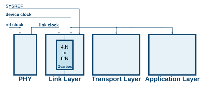
The gearbox ratio corresponds with the ratio of the link layer interface data width towards physical layer and transport layer in octets. The interface width towards the physical layer in 8B/10B (204B) mode depends on the DATA_PATH_WIDTH synthesis parameter, and can be either 4 octets (default) or 8 octets. In 204B mode the util_adxcvr supports only data width of 4 octets. In 64b66b (aka 204C) mode the data width towards the physical interface is always 8 octets.
The data path width towards the transport layer is defined by the TPL_DATA_PATH_WIDTH synthesis parameter.
The following rules apply:
- TPL_DATA_PATH_WIDTH > = DATA_PATH_WIDTH
- TPL_DATA_PATH_WIDTH = m x F; where m is a positive integer, power of 2
The link clock and device clock ratio should be the inverse of the DATA_PATH_WIDTH : TPL_DATA_PATH_WIDTH ratio.
In this context the link clock will be lane rate/40 or lane rate/80 for 204B depending on DATA_PATH_WIDTH and lane rate / 66 for 204C 64B/66B, however the device clock could vary based in the F parameter.
Software Support
To ensure correct operation it is highly recommended to use the Analog Devices provided JESD204B software packages for interfacing the peripheral. Analog Devices is not able to provide support in case issues arise from using custom low-level software for interfacing the peripheral.
Restrictions
During the design of the peripheral the deliberate decision was made to support only a subset of the features mandated by the JESD204B standard for transmitter logic devices. The reasoning here is that the peripheral has been designed to interface to Analog Devices JESD204B DAC converter devices and features that are either not required or not supported by those converter devices would otherwise lie dormant in peripheral and never be used. Instead the decision was made to not implement those unneeded features even when the JESD204B standard requires them for general purpose JESD204B transmitter logic devices. As Analog Devices DAC converter devices with new requirements are released the peripheral will be adjusted accordingly.
This approach allows for a leaner design using less resources, allowing for lower pipeline latency and a higher maximum device clock frequency.
The following lists where the peripheral deviates from the standard:
- No subclass 2 support. JESD204B subclass 2 has due to its implementation details restricted applicability and is seldom a viable option for a modern high-speed data converter system. To achieve deterministic latency it is recommend to use subclass 1 mode.
- Reduced number of octets-per-frame settings. The JESD204B standard allows for any value between 1 and 256 to be used for the number of octets-per-frame.
- The following octets-per-frame values are supported by the peripheral: 1, 2, 4 and 8.(No longer applies starting from 1.06.a)
- Reduced number of frames-per-multi-frame settings. The following values are supported by the peripheral: 1-32, with the additional requirement that F*K is a multiple of 4. In addition F*K needs to be in the range of 4-256.
- Alignment character replacement when scrambling is disabled supported starting from 1.06.a
Supported Devices
JESD204B Digital-to-Analog Converters
- AD9135: Dual, 11-Bit, high dynamic, 2.8 GSPS, TxDAC+® Digital-to-Analog Converter
- AD9136: Dual, 16-Bit, 2.8 GSPS, TxDAC+® Digital-to-Analog Converter
- AD9144: Quad, 16-Bit, 2.8 GSPS, TxDAC+® Digital-to-Analog Converter
- AD9152: Dual, 16-Bit, 2.25 GSPS, TxDAC+ Digital-to-Analog Converter
- AD9154: Quad, 16-Bit, 2.4 GSPS, TxDAC+® Digital-to-Analog Converter
- AD9161: 11-Bit, 12 GSPS, RF Digital-to-Analog Converter
- AD9162: 16-Bit, 12 GSPS, RF Digital-to-Analog Converter
- AD9163: 16-Bit, 12 GSPS, RF DAC and Digital Upconverter
- AD9164: 16-Bit, 12 GSPS, RF DAC and Direct Digital Synthesizer
- AD9172: Dual, 16-Bit, 12.6 GSPS RF DAC with Channelizers
- AD9173: Dual, 16-Bit, 12.6 GSPS RF DAC with Channelizers
- AD9174: Dual, 16-Bit, 12.6 GSPS RF DAC and Direct Digital Synthesizer
- AD9175: Dual, 11-Bit/16-Bit, 12.6 GSPS RF DAC with Wideband Channelizers
- AD9176: Dual, 16-Bit, 12.6 GSPS RF DAC with Wideband Channelizers
JESD204B RF Transceivers
- AD9371: SDR Integrated, Dual RF Transceiver with Observation Path
- AD9375: SDR Integrated, Dual RF Transceiver with Observation Path and DPD
- ADRV9009: SDR Integrated, Dual RF Transceiver with Observation Path
- ADRV9008-1: SDR Integrated, Dual RF Receiver
- ADRV9008-2: SDR Integrated, Dual RF Transmitter with Observation Path
JESD204B/C Mixed-Signal Front Ends
Technical Support
Analog Devices will provide limited online support for anyone using the core with Analog Devices components (ADC, DAC, Clock, etc) via the EngineerZone under the GPL license. If you would like deterministic support when using this core with an ADI component, please investigate a commercial license. Using a non-ADI JESD204 device with this core is possible under the GPL, but Analog Devices will not help with issues you may encounter.
More Information
resources/fpga/peripherals/jesd204/axi_jesd204_tx.txt · Last modified: 23 Jan 2024 10:37 by Adrian Costina