


This version is outdated by a newer approved version. This version (13 May 2019 15:52) is a draft.
Approvals: 0/1
This version (13 May 2019 15:52) is a draft.Approvals: 0/1
This is an old revision of the document!
Table of Contents
Distributed Control System (DCS) Demo
General Description/Overview
The distributed control system demo is a demo that uses a EVAL-ADICUP3029 connected with an EVAL-CN0416-ARDZ and up to 4 EVAL-CN0414-ARDZ or EVAL-CN0418-ARDZ boards stacked together. This system forms a MODBUS slave device that can be addressed by any MODBUS master. The EVAL-CN0414-ARDZ and EVAL-CN0418-ARDZ boards function as HART enabled inputs and outputs respectively, the EVAL-ADICUP3029 is the controller that implements the MODBUS slave and EVAL-CN0416-ARDZ is an adapter from the UART voltage levels to the RS485 levels.
MODBUS is the most popular industrial communication protocol being used today. It is a serial master-slave protocol where the master uses a set of standard commands to read and write registers on the slave device. Reading a slave register can give information about the state and inputs of the slave and writing registers can change the state or outputs of the slave. As such, there are four types of standard registers in the MODBUS slave:
| Coil/Register Number | Data addresses | Types | Names |
|---|---|---|---|
| 1 - 9999 | 0 to 270E | Read-Write | Discreet Output Coils |
| 10001 - 19999 | 0 to 270E | Read-Only | Discreet Input Contacts |
| 30001 - 39999 | 0 to 270E | Read-Only | Analog Input Registers |
| 40001 - 49999 | 0 to 270E | Read-Write | Output Holding Registers |
Each of these registers have a 16-bit address and a 16-bit value.
The Discreet Output Coils are registers that control a single output wire that has a binary value (high or low). Reading this register returns the output value of the bit and writing to it will update the coil with either low value, for writing 0, or high value, for writing anything else. The Discreet Input Contacts are registers that represent the value of a single input logic wire. The register can be only read and it is 0 if the wire is logic low and 0XFFFF if the wire is logic high. The Analog Input Registers represent an analogical value, usually from an analog wire. This register can be only read and returns a 16-bit value. The Output Holding Registers are registers that control an analogical output or a state of the slave. Reading this register returns the state of a process or an output and writing to it may change them or start a process.
Each register can be accessed using a function code:
| Function code | Action | Table name |
|---|---|---|
| 1 (0x01) | Read | Discreet Output Coils |
| 5 (0x05) | Write Single | Discreet Output Coils |
| 15 (0x0F) | Write Multiple | Discreet Output Coils |
| 2 (0x02) | Read | Discreet Input Contacts |
| 4 (0x04) | Read | Analog Input Registers |
| 3 (0x03) | Read | Output Holding Registers |
| 6 (0x06) | Write Single | Output Holding Registers |
| 16 (0x10) | Write Multiple | Output Holding Registers |
Demo Requirements
 ! - update link
The following is a list of items needed in order to replicate this demo.
- Hardware
- EVAL-ADICUP3029
- EVAL-CN0414-ARDZ and/or EVAL-CN0418-ARDZ, up to 4 boards total, in any configuration
- EVAL-CN0416-ARDZ (not needed with CLI implementation)
- Mirco USB to USB cable
- PC or Laptop with a USB port
- Software
- CrossCore Embedded Studio (2.8.0 or higher)
- ADuCM302x DFP (3.2.0 or higher)
- ADICUP3029 BSP (1.1.0 or higher)
- Serial Terminal Program (Required for running in CLI mode only)
- Such as Putty or Tera Term
Setting up the Hardware
Depending on the PLC/DCS Node configuration the power needs to be provided as follow:
- If the PLC/DCS Node contain at least a CN0418 board, then the power will be provided through any CN0418 board (the jumper for P17 MUST to be placed for each board).
- If the PLC/DCS Node contain only CN0414 boards, then the power can be provided through any CN0414 board.
PLC System block diagram

PLC System Setup Configuration
- Verify the setup configuration when possible
| MODBUS Master Interface Configuration |
||||||
|---|---|---|---|---|---|---|
| ADALM-UARTJTAG Setup | ||||||
| IO2 configuration | Mode: Push-Pull, Alternate Function: RS-485, Active High | |||||
| CN0416 Setup | ||||||
| Isolated Full Duplex | Isolated Half Duplex | Non-Isolated Full Duplex | Non-isolated Half Duplex | |||
| S1 position | NA | NA | NA | NA | ||
| S2 position | 2 | 1 | 4 | 3 | ||
| S4 position | NA | NA | 2 | 1 | ||
| S5 position | 2 | 1 | NA | NA | ||
| S6 position | NA | NA | 2 | 2 | ||
| S7 position | 2 | 2 | NA | NA | ||
| EVAL-ADICUP3029 | ||||||
| S2 position | USB position | |||||
| S5 position | WALL/USB position | |||||
| PLC System Configuration |
||||||
| CN0416 Setup | ||||||
| Isolated Full Duplex | Isolated Half Duplex | Non-Isolated Full Duplex | Non-isolated Half Duplex | |||
| S1 position | Any position | |||||
| S2 position | 2 | 1 | 4 | 3 | ||
| S4 position | NA | NA | 2 | 1 | ||
| S5 position | 2 | 1 | NA | NA | ||
| S6 position | NA | NA | 2 | 2 | ||
| S7 position | 2 | 2 | NA | NA | ||
| CN0414 Setup (if available) | ||||||
| P1 position | Any position from MULTI configuration | |||||
| P2 position | ||||||
| P10 position | Any position to result a different EEPROM address from board to board | |||||
| P11 position | ||||||
| P12 position | ||||||
| JP1 position | MULTI configuration position | |||||
| CN0418 Setup (if available) | ||||||
| P10 position | Any position from MULTI configuration | |||||
| P9 position | ||||||
| JP2 position | Any position to result a different EEPROM address from board to board | |||||
| JP3 position | ||||||
| JP4 position | ||||||
| JP1 position | MULTI configuration position | |||||
| P17 position | Jumper should be placed to power the whole system | |||||
| EVAL-ADICUP3029 | ||||||
| S2 position | ARDUINO position | |||||
| S5 position | WALL/USB position | |||||
DCS System block diagram

DCS System Setup Configuration
- Verify the setup configuration when possible
| MODBUS Master Interface Configuration |
||||||
|---|---|---|---|---|---|---|
| ADALM-UARTJTAG Setup | ||||||
| IO2 configuration | Mode: Push-Pull, Alternate Function: RS-485, Active High | |||||
| CN0416 Setup | ||||||
| Isolated Full Duplex | Isolated Half Duplex | Non-Isolated Full Duplex | Non-isolated Half Duplex | |||
| S1 position | NA | NA | NA | NA | ||
| S2 position | 2 | 1 | 4 | 3 | ||
| S4 position | NA | NA | 2 | 1 | ||
| S5 position | 2 | 1 | NA | NA | ||
| S6 position | NA | NA | 2 | 2 | ||
| S7 position | 2 | 2 | NA | NA | ||
| EVAL-ADICUP3029 | ||||||
| S2 position | USB position | |||||
| S5 position | WALL/USB position | |||||
| DCS First Node System Configuration |
||||||
| CN0416 Setup | ||||||
| Isolated Full Duplex | Isolated Half Duplex | Non-Isolated Full Duplex | Non-isolated Half Duplex | |||
| S1 position | Any position but different from node to node | |||||
| S2 position | 2 | 1 | 4 | 3 | ||
| S4 position | NA | NA | 2 | 1 | ||
| S5 position | 2 | 1 | NA | NA | ||
| S6 position | NA | NA | 2 | 2 | ||
| S7 position | 2 | 2 | NA | NA | ||
| CN0414 Setup (if available) | ||||||
| P1 position | Any position from MULTI configuration | |||||
| P2 position | ||||||
| P10 position | Any position to result a different EEPROM address from board to board | |||||
| P11 position | ||||||
| P12 position | ||||||
| JP1 position | MULTI configuration position | |||||
| CN0418 Setup (if available) | ||||||
| P10 position | Any position from MULTI configuration | |||||
| P9 position | ||||||
| JP2 position | Any position to result a different EEPROM address from board to board | |||||
| JP3 position | ||||||
| JP4 position | ||||||
| JP1 position | MULTI configuration position | |||||
| P17 position | Jumper should be placed to power the whole system | |||||
| EVAL-ADICUP3029 | ||||||
| S2 position | ARDUINO position | |||||
| S5 position | WALL/USB position | |||||
| DCS Middle Node(s) System Configuration (up to 14 nodes) |
||||||
| CN0416 Setup | ||||||
| Isolated Full Duplex | Isolated Half Duplex | Non-Isolated Full Duplex | Non-isolated Half Duplex | |||
| S1 position | Any position but different from node to node | |||||
| S2 position | 2 | 1 | 4 | 3 | ||
| S4 position | NA | NA | 2 | 1 | ||
| S5 position | 2 | 1 | NA | NA | ||
| S6 position | NA | NA | 1 | 1 | ||
| S7 position | 1 | 1 | NA | NA | ||
| CN0414 Setup (if available) | ||||||
| P1 position | Any position from MULTI configuration | |||||
| P2 position | ||||||
| P10 position | Any position to result a different EEPROM address from board to board | |||||
| P11 position | ||||||
| P12 position | ||||||
| JP1 position | MULTI configuration position | |||||
| CN0418 Setup (if available) | ||||||
| P10 position | Any position from MULTI configuration | |||||
| P9 position | ||||||
| JP2 position | Any position to result a different EEPROM address from board to board | |||||
| JP3 position | ||||||
| JP4 position | ||||||
| JP1 position | MULTI configuration position | |||||
| P17 position | Jumper should be placed to power the whole system | |||||
| EVAL-ADICUP3029 | ||||||
| S2 position | ARDUINO position | |||||
| S5 position | WALL/USB position | |||||
| DCS End Node System Configuration |
||||||
| CN0416 Setup | ||||||
| Isolated Full Duplex | Isolated Half Duplex | Non-Isolated Full Duplex | Non-isolated Half Duplex | |||
| S1 position | Any position but different from node to node | |||||
| S2 position | 2 | 1 | 4 | 3 | ||
| S4 position | NA | NA | 2 | 1 | ||
| S5 position | 2 | 1 | NA | NA | ||
| S6 position | NA | NA | 2 | 2 | ||
| S7 position | 2 | 2 | NA | NA | ||
| CN0414 Setup (if available) | ||||||
| P1 position | Any position from MULTI configuration | |||||
| P2 position | ||||||
| P10 position | Any position to result a different EEPROM address from board to board | |||||
| P11 position | ||||||
| P12 position | ||||||
| JP1 position | MULTI configuration position | |||||
| CN0418 Setup (if available) | ||||||
| P10 position | Any position from MULTI configuration | |||||
| P9 position | ||||||
| JP2 position | Any position to result a different EEPROM address from board to board | |||||
| JP3 position | ||||||
| JP4 position | ||||||
| JP1 position | MULTI configuration position | |||||
| P17 position | Jumper should be placed to power the whole system | |||||
| EVAL-ADICUP3029 | ||||||
| S2 position | ARDUINO position | |||||
| S5 position | WALL/USB position | |||||
CLI Setup block diagram

CLI Setup Configuration
The CLI system does not need the EVAL-CN0416-ARDZ board and is not affected by it's presence either.
| EVAL-ADICUP3029 | |
|---|---|
| S2 position | USB position |
| S5 position | WALL/USB position |
Configuring the Software
The software can be set up to work in CLI debug mode or in MODBUS mode. To set this make sure the relevant define in the config.h file is uncommented and the other one is commented:
//#define CLI_INTEFACE
//#define MODBUS_INTERFACE
Outputting Data
There are two interfaces available for this application: a Command Line Interface (CLI) used mainly for debugging a single PLC node and a MODBUS interface used for PLC/DCS operation for single and multiple nodes.
The CLI is implemented through UART and must be connected to a computer via USB cable. A serial terminal program must run on the host PC to display data and control the application.
The MODBUS is connected through the EVAL-CN0416-ARDZ UART to RS485 adapter and must communicate with a MODBUS master on the RS485 line.
Command Line Interface
Serial Terminal Output
A serial terminal is an application that runs on a PC or laptop that is used to display data and interact with a connected device (including many of the Circuits from the Lab reference designs). The device's UART peripheral is most often connected to a UART to USB interface IC, which appears as a traditional COM port on the host PC/ laptop. (Traditionally, the device's UART port would have been connected to an RS-232 line driver / receiver and connected to the PC via a 9-pin or 25-pin serial port.) There are many open-source applications, and while there are many choices, typically we use one of the following:
Before continuing, please make sure you download and install one of the above programs.
There are several parameters on all serial terminal programs that must be setup properly in order for the PC and the connected device to communicate. Below are the common settings that must match on both the PC side and the connected UART device.
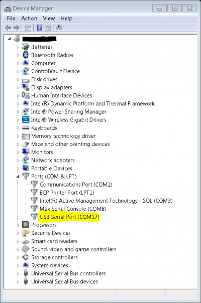
- COM Port - This is the physical connection made to your PC or Laptop, typically made through a USB cable but can be any serial communications cable. You can determine the COM port assigned to your device by visiting the device manager on your computer. Another method for identifying which COM port is associated with a USB-based device is to look at which COM ports are present before plugging in your device, then plug in your device, and look for a new COM port.
- Baud Rate - This is the speed at which data is being transferred from the connected device to your PC. These parameters must be the same on both devices or data will be corrupted. The default setting for most of the reference designs in 115200.
- Data Bits - The number of data bits per transfer. Typically UART transmits ASCII codes back to the serial port so by default this is almost always set to 8-Bits.
- Stop Bits - The number of “stop” conditions per transmission. This usually set to 1, but can be set to 2 for redundancy.
- Parity - Is a way to check for errors during the UART transmission. Unless otherwise specified, set parity to “none”.
- Flow Control - Is a way to ensure that data lose between fast and slow devices on the same UART bus are not lost during transmission. This is typically not implemented in a simple system, and unless otherwise specified, set to “none”.
In many instances there are other options that each of the different serial terminal applications provide, such as local line echo or local line editing, and features like this can be turned on or off depending on your preferences. This setup guide will not go over all the options of each tool, but just the minor features that will make it easier to read back data from the connected devices.
Example setup using Putty
- Plug in your connected device using a USB cable or other serial cable.
- Wait for the device driver of the connected device to install on your PC or Laptop.
- Open your device manager, and find out which COM port was assigned to your device.
- Open up your serial terminal program (Putty for this example)
- Click on the serial configuration tab or window, and input the settings to match the requirements of your connected device. The default baud rate for most of the reference designs is 115200. Make sure that you use the correct baud rate for your application.
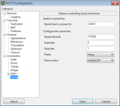
- Ensure you click on the checkboxes for Implicit CR in every LF and Implicit LF in every CF.
- Ensure that local echo and line editing are enabled, so that you can see what you type and are able to correct mistakes. (Some devices may echo typed characters - if so, you will see each typed character twice. If this happens, turn off local echo.)

- Click on the open button, and as long as your connected device and serial terminal program are setup the same, than you should see data displaying.


Hint: If you see nothing in the serial terminal, try hitting the reset button on the embedded development board.
Available Commands
Typing help or h after initial calibration sequence will display the list of commands and their short versions. The CLI mode has a board command menu which is only used to select the board. Each board present in the system has it's own command set based on the type.
Bellow is the short command list for the board menu:
| Command | Description |
|---|---|
| h | Display available commands. |
| bs | Set the active board. <board_no> = de ID of the board assigned by the program. It its displayed at the start of the program. Calling this command without an argument displays available boards again. |

The specific commands for each of the types of boards is described in they respective wiki pages:
MODBUS Interface
Because the system may contain any combination of input and output boards up to four, as a MODBUS slave, it contains two type of MODBUS registers: common and board specific.
The common registers are 5 read-only registers and 2 read-write registers. In standard MODBUS terminology that translates to 5 analog input registers and 2 holding registers:
| Name | Address | Type | Description |
|---|---|---|---|
| Detected boards | 0x0000 | Analog Input Register | Number of input and/or output boards present in the system. |
| First board data | 0x0001 | Analog Input Register | First board type (bit 0), First board CS address (bits 1,2) |
| Second board data | 0x0002 | Analog Input Register | Second board type (bit 0), Second board CS address (bits 1,2) |
| Third board data | 0x0003 | Analog Input Register | Third board type (bit 0), Third board CS address (bits 1,2) |
| Fourth board data | 0x0004 | Analog Input Register | Fourth board type (bit 0), Fourth board CS address (bits 1,2) |
| Update rate MSW | 0x00FE | Output Holding Register | Most significant word of the update rate. |
| Update rate LSW | 0x00FF | Output Holding Register | Least significant word of the update rate. |
The board type bit is “0” for CN0414 and “1” for CN0418.
The update rate is stored as:
  Update rate MSW = ((Actual update rate * 10000) & 0xFFFF0000) >> 16;
  Update rate LSW = ((Actual update rate * 10000) & 0x0000FFFF) >> 0;
So the equation used to retrieve the update rate is:
Or in code form:
Actual update rate = (((Update rate MSW << 16) & 0xFFFF0000) | Update rate LSW) / 10000;
Adding a board to the system adds a number of board specific registers: 50 analog input registers and 7 output holding registers for adding an EVAL-CN0414-ARDZ, and 30 analog input registers and 10 output holding registers for adding an EVAL-CN0418-ARDZ.
As stated before, adding an EVAL-CN0414-ARDZ adds 57 registers to the device: 50 analog input registers and 7 output holding registers. The analog input registers are: 16 for ADC input values, 4 for ADC input open wire detection flags and 50 for HART receive buffer. The output holding registers are: 1 for ADC output coding, 1 for ADC filter options, 1 for ADC postfilter options, 1 for ADC output data rate options, 1 for ADC open wire detection enable, 1 for HART command zero and 1 for HART channel select. The output holding registers are: 16 for the channel registers, 4 for Open Wire Detection and 30 for the HART input buffer. Adding an EVAL-CN0418-ARDZ adds 40 registers: 30 analog input registers and 10 output holding registers. There are 30 HART input registers as analog input registers. The output holding registers are: 4 for channel ranges (one for each channel), 4 for the channels output (one for each channel), 1 for the HART active channel and 1 for the HART command zero.
Note that being a dynamic system the registers presented below do not have an unique address, but have an address offset that can be used to calculate their address. The function is:
Address = (ADC_CS_address << 12) + (MODBUS_slave_address << 8) + Address_offset;
Register map for the EVAL-CN0414-ARDZ:
| Name | Address Offset | Type | Description |
|---|---|---|---|
| Channel 1 MSW | 0x05 | Analog Input Register | Most significant word of the first ADC channel. |
| Channel 1 LSW | 0x06 | Analog Input Register | Least significant word of the first ADC channel. |
| Channel 2 MSW | 0x07 | Analog Input Register | Most significant word of the second ADC channel. |
| Channel 2 LSW | 0x08 | Analog Input Register | Least significant word of the second ADC channel. |
| … | … | … | … |
| Channel 8 MSW | 0x13 | Analog Input Register | Most significant word of the eighth ADC channel. |
| Channel 8 LSW | 0x14 | Analog Input Register | Least significant word of the eighth ADC channel. |
| Channel 1 OWD | 0x15 | Analog Input Register | Open wire detection flag of the first voltage channel. |
| Channel 2 OWD | 0x16 | Analog Input Register | Open wire detection flag of the second voltage channel. |
| Channel 3 OWD | 0x17 | Analog Input Register | Open wire detection flag of the third voltage channel. |
| Channel 4 OWD | 0x18 | Analog Input Register | Open wire detection flag of the fourth voltage channel. |
| HART IN 1 | 0x19 | Analog Input Register | First word of the HART input buffer. |
| HART IN 2 | 0x1A | Analog Input Register | Second word of the HART input buffer. |
| … | … | … | … |
| HART IN 30 | 0x36 | Analog Input Register | 50th word of the HART input buffer. |
| ADC Output Code | 0x00 | Output Holding Register | Set the output coding for the ADC: 0 - bipolar coding (default); 1 - unipolar coding. |
| ADC Filter | 0x01 | Output Holding Register | Set the input filter for the ADC: 0 - s5+s1 (default); 1 - s3. |
| ADC Postfilter | 0x02 | Output Holding Register | Set the input postfilter for the ADC: 0 - 27 SPS, 47 dB rejection, 36.7 ms settling; 1 - 25 SPS, 62 dB rejection, 40 ms settling; 2 - 20 SPS, 86 dB rejection, 50 ms settling; 3 - 16.67 SPS, 92 dB rejection, 60 ms settling; 4 - disable postfilter (default). |
| ADC ODR | 0x03 | Output Holding Register | Set the output data rate for the ADC: [0-5] - 31250 SPS (default); 6 - 15625 SPS; 7 - 10417 SPS; 8 - 5208 SPS; 9 - 2597 SPS; 10 - 1007 SPS; 11 - 503.8 SPS; 12 - 381 SPS; 13 - 200.3 SPS; 14 - 100.5 SPS; 15 - 59.52 SPS; 16 - 49.68 SPS; 17 - 20.01 SPS; 18 - 16.63 SPS; 19 - 10 SPS; 20 - 5 SPS; 21 - 2.5 SPS; 22 - 1.25 SPS; |
| ADC OWD EN | 0x04 | Output Holding Register | Enable/disable open wire detection for the ADC: 0 - disable OWD (default); 1 - enable OWD. |
| HART cmd 0 | 0x05 | Output Holding Register | Writing “1” to this register sends HART command 0 then the register resets to “0”. |
| HART CH select | 0x06 | Output Holding Register | Select enable a current channel for HART communication: 0 - Channel 1 (default); 1 - Channel 2; 2 - Channel 3; 3 - Channel 4. |
Register map for the EVAL-CN0418-ARDZ:
| Name | Address Offset | Type | Description |
|---|---|---|---|
| HART IN 1 | 0x05 | Analog Input Register | First word of the HART input buffer. |
| HART IN 2 | 0x06 | Analog Input Register | Second word of the HART input buffer. |
| … | … | … | … |
| HART IN 30 | 0x22 | Analog Input Register | 50th word of the HART input buffer. |
| Channel 1 range | 0x00 | Output Holding Register | Output range for the first DAC channel: 0 - 0V to 5V; 1 - 0V to 10V; 2 - -5V to 5V; 3 - -10V to 10V; 4 - 4ma to 20ma; 5 - 0ma to 20ma; 6 - 0ma to 24ma. |
| Channel 2 range | 0x01 | Output Holding Register | Output range for the second DAC channel: 0 - 0V to 5V; 1 - 0V to 10V; 2 - -5V to 5V; 3 - -10V to 10V; 4 - 4ma to 20ma; 5 - 0ma to 20ma; 6 - 0ma to 24ma. |
| Channel 3 range | 0x02 | Output Holding Register | Output range for the third DAC channel: 0 - 0V to 5V; 1 - 0V to 10V; 2 - -5V to 5V; 3 - -10V to 10V; 4 - 4ma to 20ma; 5 - 0ma to 20ma; 6 - 0ma to 24ma. |
| Channel 4 range | 0x03 | Output Holding Register | Output range for the fourth DAC channel: 0 - 0V to 5V; 1 - 0V to 10V; 2 - -5V to 5V; 3 - -10V to 10V; 4 - 4ma to 20ma; 5 - 0ma to 20ma; 6 - 0ma to 24ma. |
| Channel 1 | 0x04 | Output Holding Register | Output code of the first DAC channel. |
| Channel 2 | 0x05 | Output Holding Register | Output code of the second DAC channel. |
| Channel 3 | 0x06 | Output Holding Register | Output code of the third DAC channel. |
| Channel 4 | 0x07 | Output Holding Register | Output code of the fourth DAC channel. |
| HART cmd 0 | 0x08 | Output Holding Register | Writing “1” to this register sends HART command 0 then the register resets to “0”. |
| HART CH select | 0x09 | Output Holding Register | Select enable a current channel for HART communication: 0 - Channel A (default); 1 - Channel B; 2 - Channel C; 3 - Channel D. |
qModMaster Example
| Common analog input registers read | |
| Reading these registers with 2 EVAL-CN0414-ARDZ and 2 EVAL-CN0418-ARDZ connected to the system it can be seen that 4 boards are found at address “0000”. |  |
| The next address read “0001” indication that the board is a EVAL-CN0418-ARDZ and has address 0; | |
| The second address reads “0003” indication that the board is EVAL-CN0418-ARDZ and has the address 1; | |
| The third register read “0004” indicating that the board is EVAL-CN0414-ARDZ and has address 2; | |
| And the last register reads “0006” for EVAL-CN0414-ARDZ and address 3. | |
| ADC channels of one of the input boards with MODBUS | |
| The second read shows the input channels data for the last input board found. This is done by reading 16 analog input registers fount at address 0x3105. |  |
| ADC change the output code | |
| This is an example on how to change the ADC output code of the third board (input board with address 3) by writing the output holding register at the address 0x3100. |  |
 |
|
MinimalModbus basic examples
In this application, the instrument is connected via a USB to RS485 bridge.
For example, consider an instrument (slave) with Modbus RTU and address number 1 to which we are to communicate via a serial port with the name COM12. The instrument stores the actual configuration in registers 0 to 4. To read data from the instrument:
- read_common_analog_input_registers.py
"""Read common analog input registers to determine PLC/DCS configuration."""

import minimalmodbus

# declare an instrument object with port name, slave address as input arguments
INSTRUMENT = minimalmodbus.Instrument('COM12', 1)

# read 5 registers starting from address 0 by using function code 4
COMMON_ANALOG_INPUT_REGISTERS = INSTRUMENT.read_registers(
    registeraddress=0, numberOfRegisters=5, functioncode=4)

# result a list with 5 elements in decimal format
print(COMMON_ANALOG_INPUT_REGISTERS)
[4, 1, 3, 4, 6]
In this example, after we run the above piece of code it results that we have 4 boards connected. Two of this boards are EVAL-CN0414-ARDZ and other two are EVAL-CN0418-ARDZ. The EVAL-CN0414-ARDZ boards have address 0b10 and 0b11 while EVAL-CN0418-ARDZ boards have address 0b00 and 0b01.
Next, if we want to read all analog input channels from one EVAL-CN0414-ARDZ we can use the following:
- read_adc_analog_input_registers.py
"""Read analog input registers to determine ADC channels code."""

import minimalmodbus

# declare an instrument object with port name, slave address as input arguments
INSTRUMENT = minimalmodbus.Instrument('COM12', 1)

# read 16 registers starting from address 12549 by using function code 4
ADC_CHANNELS_CODES = INSTRUMENT.read_registers(
    registeraddress=12549, numberOfRegisters=16, functioncode=4)

# result a list with 16 elements in decimal format
print(ADC_CHANNELS_CODES)
[127, 65158, 127, 65514, 127, 65194, 127, 64995, 127, 65285, 127, 65244, 127, 65292, 127, 65278]
In this example, after we run the above piece of code it results a list of 16 elements in decimal format. First 8 values corespond to voltage channels and last to current channels.
Next, if we want to change the output code of one EVAL-CN0414-ARDZ ADC to be unipolar instead of bipolar we can use the following:
- set_adc_output_code.py
"""Read and write one output holding register to change ADC output code."""

import minimalmodbus

# declare an instrument object with port name, slave address as input arguments
INSTRUMENT = minimalmodbus.Instrument('COM12', 1)

# read a single register from address 12544 by using function code 3
INITIAL_ADC_OUTPUT_CODE = INSTRUMENT.read_register(
    registeraddress=12544, functioncode=3)

# result an integer
print(INITIAL_ADC_OUTPUT_CODE)

# wrie a single register from address 12544 by using function code 6
INSTRUMENT.write_register(registeraddress=12544, value=1, functioncode=6)

# read a single register from address 12544 by using function code 3
FINAL_ADC_OUTPUT_CODE = INSTRUMENT.read_register(
    registeraddress=12544, functioncode=3)

# result an integer
print(FINAL_ADC_OUTPUT_CODE)
0
1
In this example, after we run the above piece of code it results an integer which coresponds to ADC coding format. The default value 0, indicate that the ADC is set to bipolar coding format, while a value of 1 will indicate an unipolar coding format.
Obtaining the Source Code
We recommend not opening the project directly, but rather import it into CrossCore Embedded Studios and make a local copy in your workspace.
The source code and include files of the ADuCM3029_demo_cn0435 can be found here:
! - update link
How to use the Tools
The official tool we promote for use with the EVAL-ADICUP3029 is CrossCore Embedded Studio. For more information on downloading the tools and a quick start guide on how to use the tool basics, please check out the Tools Overview page.
Importing
For more detailed instructions on importing this application/demo example into the CrossCore Embedded Studios tools, please view our How to import existing projects into your workspace section.
Debugging
For more detailed instructions on importing this application/demo example into the CrossCore Embedded Studios tools, please view our How to configure the debug session section.
Project Structure
The application controls a dynamic system that can be physically different every time it is run. to do this it has two parts:
- The system initialization.
- The system main process.

After getting parameters of the system supplied by the user in code the program initializes the software modules common to all the boards: I2C, UART, SPI, microcontroller power, software UART and the AD5700 HART modem. If the MODBUS interface is used, the update timer for the input boards is also initialized in this stage as a common module. If, by comparison, the CLI is used, each input board present initializes its own version of the update timer driver.
After these initializations the system runs a board discovery routine. By using the presence of I2C EEPROM memory and testing the SPI configuration, all boards in the system are discovered and labeled as either CN0414 or CN0418. If the MODBUS interface is used, the system also scans for its MODBUS slave address and maps and initializes MODBUS registers.
After board discovery, if the CLI is used, no board is set as active and the system manager loads the main menu process. If the MODBUS is used, the system activates the first board it discovers.

CLI Process
If the CLI is used, no board is active after the initialization and the system stands by to receive commands. If the user sets one of the boards to be active, the program loads the commands and process specific to that board and starts sunning them until the application is stopped or the “exit” command is called.

MODBUS Interface Process
If the MODBUS interface is used the first board discovered is the active board. If it is a CN0414 the program runs its process until all channels are updated. If it is a CN0418 the program runs its process only once. After this the system deactivates the board and activates the next board discovered until all the boards have been active and updated. The system than cycles back from the beginning.
Meanwhile the system scans the MODBUS channel for commands and if one is found that is addressed to this node it executes it and sends back a response.

Board Specific Processes
The process and commands for each type of boards is described in the appropriate application page:
End of Document
resources/eval/user-guides/eval-adicup3029/reference_designs/demo_plc_modbus.1557755576.txt.gz · Last modified: 13 May 2019 15:52 by Mihai Ionut Suciu