


This version (08 Mar 2024 12:15) was approved by Zaeefa Pandangan.The Previously approved version (08 Mar 2024 09:26) is available.
Table of Contents
Evaluating the AD9106/AD9102 Digital-to-Analog and Waveform Generator Converter using MBED
Navigation
You can return to Homepage here: AD9106 & AD9102 Evaluation Boards
Preface
Analog Devices is an Mbed Partner and develops code on the platform for multiple products. The AD9106 and AD9102 Mbed-enabled evaluation boards and example Mbed codes can be used as starting point for characterizing the high-speed waveform generator digital-to-analog converters before integrating them into specific applications.
This guide will focus on how AD9106-ARDZ-EBZ/AD9102-ARDZ-EBZ works with SDP-K1 controller board and example Mbed program developed by Analog Devices. Multichip synchronization evaluation using two AD910x-ARDZ-EBZ is also discussed. Users are not limited to using SDP-K1 for evaluation or prototyping. The evaluation boards and the example codes with minor changes can work with other ARM-based Mbed-enabled boards. User interface is text-based.
The evaluation setup can be powered by USB only and does not require a high-frequency waveform generator for clock input. The evaluation board has an on-board 156.25 MHz crystal oscillator. To evaluate multichip synchronization, however, a common external clock is needed. To fit the evaluation system in a small form factor and manage power consumption within USB specifications, AD9106 and AD9102 supply voltages AVDD, DVDD and CLKVDD are limited to 3.3V only.
Tip: Click on any picture in this guide to open an enlarged version.
Software Needed
Useful Links
Quick Start Guide
Single-Board Evaluation
- Attach the AD9106-ARDZ-EBZ / AD9102-ARDZ-EBZ evaluation board to SDP-K1. Make sure that SDP-K1 VIO is set to 3.3V through the P14 jumper by placing the shunt on the center and 3.3V pins. Refer to Figure 1 below.
 Figure 1. SDP-K1 VIO Configuration
Note: If the VIO is set to 1.8V, 0xFFFF will be read from all registers and any change in their data cannot be applied.
- Connect SDP-K1 to PC over USB. DS1 and DS2 on SDP-K1 and DS1 on the evaluation board should light up. If DAC outputs are connected to the on-board amplifiers, connect a 7-V-to-12-V, 30-W wall wart to SDP-K1 DC jack or to P15 on the evaluation board.
- Connect the outputs of the evaluation board to an oscilloscope using SMA-to-BNC cables. Apply one of the oscilloscope settings shown in the waveform captures of the example patterns in Figures 9a to 9b and Figures 10a to 10c.
- Go to the EVAL-AD910x example code in GitHub repository and copy its HTTPS URL through the Code dropdown button as shown in Figure 2. Log on to https://studio.keil.arm.com/ and import the codes by going to File > Clone… then pasting the repository link in the URL field of the Clone window as depicted in Figure 3. Make sure to input the desired Project name and tick the Make this active project checkbox before clicking the Add project button.
 Figure 2. EVAL-AD910x Mbed Code Repository in GitHub
 Figure 3. Importing the Project to Keil Studio Cloud
- In Keil Studio Cloud, configure the following settings under File > Preferences, as shown in Figure 4:
- Select cmsis for Flash Mode.
- Clear the Verify the contents downloaded to flash checkbox under Verify Flash.
 Figure 4. Configuring Flash Settings in Keil Studio Cloud Preferences
- To connect the device to Keil Studio Cloud, configure the following settings in the Explorer sidebar menu, as shown in Figure 5:
- Build Target: SDP-K1
- Connected Device: SDP-K1: <Device Number>
 Figure 5. Configuring Explorer Sidebar Menu Settings
- Open config.h and define the ACTIVE_DEVICE as in Figure 6. If the evaluation board in use is AD9102-ARDZ-EBZ, uncomment line 27 by deleting the two forward slashes. Otherwise, keep line 27 commented.
 Figure 6. Selecting the active device through config.h
- Open main.cpp and set the code for single-board evaluation by uncommenting line 90 as seen in Figure 7.
 Figure 7. Setting the Code for Single-/Multi-Board Evaluation
- As shown in Figure 8, click the Open serial monitor button, connect to the correct serial port through the browser popup, then select 115200 as the baud rate in the Keil Studio dropdown list.
 Figure 8. Running the Project
- Go back to Explorer then click the Run project button to program, flash, and reset the device. The Run terminal will automatically be opened and display in real-time the status of loading the program onto the controller.
Note: DS1 in SDP-K1 will blink during the flashing process.
- After flashing, open the serial monitor window to configure the AD910x-ARDZ-EBZ board.
- Follow the program instructions that will appear on the serial monitor window. If the device’s clock inputs are connected to the on-board crystal oscillator and the DAC outputs to the RF transformers (default), press any key other than y for each of the first two questions. Refer to Figures 9a and 9b.


Figure 9a. EVAL-AD9106 Demo Program Menu (Single-Board) | Figure 9b. EVAL-AD9102 Demo Program Menu (Single-Board)
- Choose an example (AD9102) or a set of examples (AD9106) from the menu by entering its corresponding number (see Figure 10). Recommended examples for the default hardware configuration are options 3 and 5 for AD9106 and options 3, 5, and 6 for AD9102. To observe waveforms with frequency components outside the RF transformer’s bandwidth of 0.5-600 MHz, connect the DAC outputs to the on-board amplifiers.
 Figure 10. Selecting examples and printing of SPI register addresses and data on the serial monitor (Single-Board Evaluation)
- After selecting a pattern/set of patterns, the device’s register addresses with their corresponding data words will be displayed on the console and patterns will be generated at the DAC outputs as depicted in Figure 10. Sample output waveforms are shown in Figures 11a to 11b for AD9106 and Figures 12a to 12c for AD9102. For more waveform examples, see Sample Waveforms out of RF transformer and Sample Waveforms out of Onboard Amplifier.


Figure 11a. AD9106 Example 3 out of RF transformers | Figure 11b. AD9106 Example 5 out of RF transformers


Figure 12a. AD9102 Example 3 out of an RF transformer | Figure 12b. AD9102 Example 5 out of an RF transformer
 Figure 12c. AD9102 Example 6 out of an RF transformer
- After playing the selected pattern, either generate another or exit the program. If the former is selected, pattern generation will stop and program will restart like in Figure 13a. Otherwise, after terminating the program like in Figure 13b, repeat Step 10 to restart the program.


Figure 13a. Choosing another pattern (Single-Board Evaluation) | Figure 13b. Exiting the program (Single-Board Evaluation)


Multi-Board Evaluation / Multichip Synchronization Evaluation
The technical article Unlocking the Potential of Open-Source Evaluation Platforms for Prototyping Ultrasound Transmit Subsystems describes how multichip synchronization can be evaluated using AD9106-ARDZ-EBZ boards. This section presents an outline of this procedure with a step-by-step guide that includes utilizing the AD910x Mbed codes in performing the evaluation with either two AD9106-ARDZ-EBZ or two AD9102-ARDZ-EBZ boards. For additional hardware needed, see Materials section of the technical article.
- Attach one AD9106-ARDZ-EBZ / AD9102-ARDZ-EBZ evaluation board to SDP-K1 and connect the second EVAL board (should be of the same generic) to the latter through the docked EVAL board using the male-to-male connector wires following the configuration in Table 1. To synchronize the boards, make sure that both are configured for external clocking using the same clock source and that the wire connecting the TRIGGER pins is as short as possible to minimize delay between the outputs from the two boards. See the technical article for further details. Additionally, the boards should be configured to use on-board amplifiers and that the SDP-K1 VIO should be set to 3.3V through the P14 jumper by placing the shunt on the center and 3.3V pins. Refer to Figure 1.
Table 1. Pin connections between the SDP-K1 and two AD910x-ARDZ-EBZ boards
 * If Board 2 CSB pin is connected to the alternate GPIO pin (R39 is installed instead of R38)
- Connect the continuous wave generator for clock input to J10 of the two evaluation boards through the T-splitter. Set the clock input to 180 MHz and 1 dBm.
- Connect SDP-K1 to PC over USB. DS1 and DS2 on SDP-K1 and DS1 on the evaluation boards should light up. Since the DAC outputs are connected to the on-board amplifiers, a 7-V-to-12-V, 30-W wall wart should be connected to SDP-K1 DC jack or to P15 on the docked evaluation board.
- Connect the Channel 1 output of each evaluation board to an oscilloscope using SMA-to-BNC cables. Apply the oscilloscope settings shown in the waveform captures of the example patterns in Figures 16a to 16c.
- Perform Single-Board Evaluation Steps 4 to 9 to import and configure the AD910x Mbed project. In Step 8, set the code for multi-board/multichip synchronization evaluation by uncommenting line 91 as seen in Figure 7.
- Go back to Explorer then click the Run project button to program, flash, and reset the devices. The Run terminal will automatically be opened and display in real-time the status of loading the program onto the controller.
Note: DS1 in SDP-K1 will blink during the flashing process.
- After flashing, open the serial monitor window to configure the AD910x-ARDZ-EBZ boards.
- Follow the program instructions that will appear on the serial monitor window. Since the devices' DAC outputs are connected to the on-board amplifiers, press y for the first question. Refer to Figures 14a and 14b.


Figure 14a. EVAL-AD9106 Demo Program Menu (Multi-Board) | Figure 14b. EVAL-AD9102 Demo Program Menu (Multi-Board)
- Choose an example (AD9102) or a set of examples (AD9106) for each board from the menu by entering its corresponding number (see Figure 15a and Figure 15b).


Figure 15a. EVAL-AD9106 Selecting Pattern for Board 1 | Figure 15b. EVAL-AD9106 Selecting Pattern for Board 2
- After selecting a pattern/set of patterns, the device’s register addresses with their corresponding data words will be displayed on the console and patterns will be generated at the DAC outputs as depicted in Figure 15. Resulting waveforms are shown in Figures 16a to 16c.

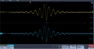
Figure 16a. Channel 1 Example 3 out of 2 AD9102 / 2 AD9106 | Figure 16b. Channel 1 Example 5 out of 2 AD9102 / 2 AD9106
 Figure 16c. Channel 1 Example 6 out of 2 AD9102 / 2 AD9106
- After playing the patterns, either generate another set or exit the program. If the former is selected, pattern generation will stop and program will restart like in Figure 17a. Otherwise, after terminating the program like in Figure 17b, repeat Step 6 to restart the program.


Figure 17a. Choosing another pattern (Multi-Board Evaluation) | Figure 17b. Exiting the program (Multi-Board Evaluation)


Using the Example Mbed Codes
The EVAL-AD910x Example Mbed Codes can be used as a starting point for developing firmware for targeted applications. The eval-ad910x codes in the ADI GitHub repository demonstrate how to set up SPI communication between the ARM-based Mbed-enabled hardware, SDP-K1, and the waveform generator DAC, AD9106/AD9102.
To import the codes to Keil Studio Cloud as discussed in the Quick Start Guide, the user should have an Arm or Mbed account and is logged on to https://studio.keil.arm.com/. After successful project import, the user is free to use and modify the codes as needed, in compliance with the terms and conditions outlined in the LICENSE file.
Each file and function has a short description/brief. This section focuses on how several files and functions can be modified using the Keil Studio Cloud.
Setting up the SPI Interface
Aside from choosing the active device as described in the Quick Start Guide, SPI protocol parameters -- particularly the clock frequency -- can be set at the application-level codes. Word length (WORD_LEN) and Polarity (POL) need not be changed and are already set for AD9106 and AD9102. Refer to Mbed OS 6 SPI Documentation for more information on these parameters.
Instructions on setting the SPI clock (SCLK) frequency are already provided in config.h as shown in Figure 18. The reason why SCLK can only be set to a number of fixed frequencies is discussed in this Mbed Wiki page: SPI output clock frequency. SPI lines out of the Arduino headers or SPI1 module of the SDP-K1 ARM processor uses a 100-MHz peripheral clock. Refer to these relevant source codes:

Figure 18. SPI protocol definitions, example SRAM vectors, and example SPI register configurations in config.h
Initialization of digital I/O pins connected to the DAC being evaluated, and declaration of SPI register addresses and device-specific functions are in ad910x.h. See Figure 19. The functions are implemented in ad910x.cpp. The Mbed platform drivers allow setup of 4-wire SPI interface. Refer to Mbed documentation for other configurations.

Figure 19. Device-specific I/O pins and functions declarations in ad910x.h
Modifying SRAM Vectors
SRAM Vectors in config.h can be easily modified for a specific application. For both AD9106 and AD9102, there are 4096 addresses in the on-chip SRAM. Word length is 14 bits for AD9102, 12 bits for AD9106, and is left-justified. For AD9102, data should be written in bits [15:2] and for AD9106 in bits [15:4] of each SRAM address.
Although the SRAM vectors can be modified manually, it will be more convenient to create new vectors using DPG Lite or Vector Generator from Analysis | Control | Evaluation (ACE) Software.
When creating data vectors for AD9106 and AD9102, make sure to choose the proper DAC resolution and leave the Unsigned Data box unchecked. Shown in Figures 20a and 20b are the types of waveforms that can be generated using DPG Lite and ACE's Vector Generator, respectively, and Figures 21a and 21b are three vectors with a combined record length of 4096 generated using the same software programs which can be uploaded to the SRAM. These can be saved as text files and integrated into the source code.


Figure 20a. Waveforms that can be generated using DPG Lite | Figure 20b. Waveforms that can be generated using ACE's Vector Generator


Figure 21a. Generating waveform vectors using DPG Lite | Figure 21b. Generating waveform vectors using ACE's Vector Generator
It is not required to write to all 4096 addresses. Each DAC channel in a device can fetch data from a fixed SRAM address to another. The start and stop addresses can be set using the following registers:
- 0x5E and 0x5F for AD9102
- 0x5E and 0x5F, 0x59 and 0x5A, 0x55 and 0x56, and 0x51 and 0x52 for AD9106 Channels 1 to 4, respectively.
SRAM data format or code follows two’s complement notation. Refer to Table 2 for the equivalent current output for an input code. 14-bit code should be shifted left by 2 bits before writing it to AD9102 SRAM while 12-bit code should be shifted left by 4 bits before writing it to AD9106 SRAM. Alternatively, 14-bit data shifted left by 2 bits can be written to AD9106 SRAM but the last two bits with be truncated. This is why in AD910x_update_sram() function in ad910x.cpp, SRAM data is by default shifted 2 bits to the left. Refer to Figure 22.
Table 2. Range of SRAM Data Values

Figure 22. Function that writes to on-chip SRAM in ad910x.cpp
AD910x_print_sram() function is declared in ad910x.h and implemented in ad910x.cpp but is by default not called in the main program main.cpp. The function can be used to print in the console n number of data words from SRAM. This can be done by calling the function in main.cpp after AD910x_update_sram().
Changing SPI Register Values
AD9106 and AD9102 have similar register maps. The latter only has less number of registers that affect device functionality because writing to registers for the three other DAC channels will only have an effect to AD9106. Nonetheless, the defined SPI registers address in ad910x.h will work for both devices.
The SPI register addresses were written as comment in config.h and aligned with example SPI register values for user’s convenience. Same as the SRAM vectors, these SPI register values can also be easily modified for specific applications. Refer to the device datasheets for the SPI register descriptions.
Power Supply Enable/Shutdown Pins
Other I/Os like the ones connected to the EN pin of the on-board oscillator supply, CVDDX, and to the SHDN_N pin of the on-board amplifier supply, LT3472, are defined in main.cpp.
As shown in Figure 23, if external or off-board clock source is chosen, en_cvddx = 0 and no power is supplied to CVDDX. If the on-board oscillator is chosen, en_cvddx = 1 and 3.3V is supplied to CVDDX.

Figure 23. Power supply enable/shutdown pins in main.cpp
If the user confirms that the DAC outputs are connected to the on-board amplifiers, shdn_n_lt3472 = 1 and 5.2V and -5.2V are supplied to the amplifiers provided a wall wart is connected to SDP-K1 or the evaluation board. Otherwise, shdn_n_lt3472 = 0 and the amplifiers are not powered up.
resources/eval/dpg/eval-ad9106-mbed.txt · Last modified: 08 Mar 2024 12:14 by Zaeefa Pandangan