


This version (03 Apr 2014 18:59) was approved by Michael Fowler, Jun Kakinuma.The Previously approved version (07 Aug 2012 14:27) is available.
Table of Contents
DPG2
The Data Pattern Generator is a bench-top instrument for driving vectors into Analog Devices' high-speed Digital-to-Analog converters. The DPG connects to a PC over USB, and allows a user to download a vector from their PC into the DPG’s internal memory. Once downloaded, the vector can be played out to an attached Evaluation Board for a specific DAC at full speed. This allows for rapid evaluation of the DAC with both generic and customer-generated test data.
Please note: Analog Devices' pattern generators and high-speed DAC evaluation boards are designed and sold solely to support an efficient and thorough means by which to evaluate Analog Devices high speed DACs in a lab environment for a wide range of end applications. Any application or use of the pattern generators and/or high-speed DAC evaluation boards, other than specified above, will not be supported.
The DPG2 has been replaced by the DPG3. For information on the software used to control the DPG2 and DPG3, see the High-Speed DAC Software Suite page.
Ordering Code
The part number for the DPG2 is AD-DAC-DPG-BZ.
Hardware Specifications
Please note that not all hardware options and specifications are supported with any particular evaluation board or software package. Specifications are subject to change without notice.
- Converter Interfaces
- CMOS Interface
- 32-bits (shared with the P lines of the LVDS bus)
- Up to 250Mbps (SDR)
- LVDS Interface
- 32-bits (P lines shared with CMOS interface)
- Up to 1.25Gbps (625MHz DDR)
- Memory
- Dual DDR2 DIMM
- Maximum pattern length of 134M samples (limited to 30M samples in most applications)
- PC Interface
- USB 2.0 “B” connector
- Clocking
- On-connector clock input for all interfaces
- Optional external clock input via SMA jack for CMOS interfaces
- Rated for operation only at 25ºC
- Multi-Unit Synchronization
- Up to four DPG2's may have their LVDS interfaces synchronized together
- Requires additional Synchronization Board and cabling

Output Data
The DPG2 has two 16-bit ports capable of interfacing with both LVDS and LVCMOS devices. When transmitting a data vector each sample from the data file is played sequentially on the output port. Note that while the two data ports are labeled “I” and “Q” in the pinout, the actual mapping of bits to DACs will depend on the particular evaluation board connected. Many DACs with interfaces of 16-bits or less will only use a single port (generally the “I” port).
For LVCMOS/LVTTL devices, 3.3V, 2.5V, and 1.8V levels are supported.
The vector length must be at least 256 points per channel, and the length must be divisible by 256 for proper operation.
Clocking
The DPG requires an input clock to set the frequency of the data output. This is labeled DCO, for Data Clock Out. In LVDS mode, this clock is supplied through the main connector, and no other cables are required. In CMOS mode, the clock can either come through the main connector, or can be supplied via the SMA jacks J12 and J13. Which method is available will depend on the design of the evaluation board. When selecting a configuration, the names ending in (DCO) will have the clock received through the main connector. Configuration names ending in (SMA) will expect a clock to be cabled into J12 or J13.
The DPG also provides an output clock, DCI, which is synchronous with the data leaving the DPG2.
Hexadecimal Display
Each DPG2 is equipped with a small red display. When a DPG2 is powered up, but not yet connected to software, the display will read 0. Once software has initiated communication with the DPG2, the display will indicate the index of the DPG2. This is used when multiple DPG2s are connected to the same PC.
The left “decimal point” on the display indicates if the DPG2 has been “configured”. If the left point is not lit, the DPG2 will need to be configured before any other operations.
The right decimal point indicates the status of the vector. The point will not be lit if a vector has not been downloaded into the DPG2. The point will stay lit when a vector is downloaded but not playing, and the point will blink when the vector is being played to the DUT.
SMA Jacks
There are two SMA jacks location on the DPG2 (J12 and J13). These are an optional input clock path for use with older CMOS interface DAC evaluation boards.
Multi-Unit Synchronization
Up to four DPG2's can be synchronized together so that the LVDS data coming out of all the DPGs is aligned to a common clock. Synchronization is not supported with the CMOS interface.
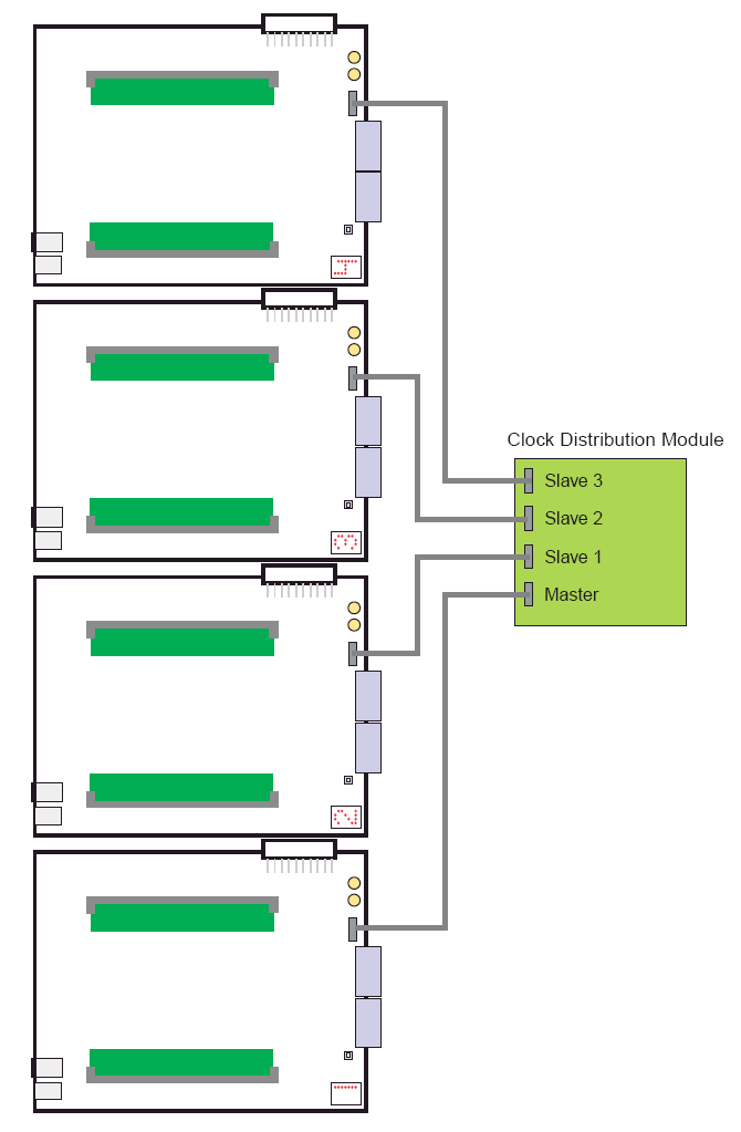
A clock distribution module (Part Number HSC-DAC-DPG-CLKDIS) is required, as well as one Samtec HQCD-030-15.00-TED-TEU-1 cable per DPG2, for synchronizing. When ordering the distribution module, please indicate how many cables are needed. A schematic of the clock distribution board is available here.
The synchronization system works by having the Master unit forward the clock it receives (from the evaluation board attached to the Master) on to the Clock Distribution Module. The module then sends this clock back out to each unit, including the Master. The trace lengths and cables are all very well matched, and ensure that the clocks arrive at each slave DPG2 at the same time. The DPG2s then use this clock, instead of the clock from their respective evaluation board, to clock the data.
This requires that all the evaluation boards be clocked with exactly the same clock, as any frequency drifts between the evaluation boards will not be seen in the data, leading to data overrun or underrun.
Setting up Multi-Unit Synchronization
1. Connect the sync cables between the DPGs (up near the main data connector) and the sync board. Power the sync board with +5V. Make sure one of the DPG2’s is connected to the “Master” connector on the sync board, the other units can be connected to any of the other outputs on the sync board.
2. Connect a DAC board up to each DPG2 as you normally would, except only connect one of the DAC eval board to USB. Power up the eval boards.
3. Configure the DAC eval board as you would like with the SPI program. Then disconnect the USB, and connect it to the next eval board, configure it, and so on until all eval boards are setup.
4. With all the DPG2s powered on and connected to USB, open DPGDownloader. It should see all the DGP2s, and have a separate “panel” for each. On the left side of each panel, there is an option that defaults to “Single”. On the Master DPG2, change this to Master, and on the others change it to Slave.
5. Import or create the vectors you want the DACs to play out, and assign them to each DAC. You can correlate each DAC in the software with the number displayed in red on the DPG2 itself.
6. Download the vectors to all the DPG2s. Hit play on all the units except the Master. This arms the slaves to be ready to transmit.
7. Hit Play on the Master unit. This starts playback on all the units.
Connector Pinouts
CMOS/LVDS Pinout
The CMOS/LVDS connection on DPG2 and DPG3 uses two AMP/Tyco 1469169-1 connectors, placed side-by-side, with 139.2mil spacing between the centers of the innermost pins on both connectors. The mating connector on the evaluation board side is two AMP/Tyco 1469028-1. Note that both connectors are always required.
Left Side Connector
The left connector when looking at the connection on the DPG from the evaluation board side (J17 on the DPG2, J8 on the DPG3)
| Pin | Name | Description |
|---|---|---|
| A1 | CLK_DCOA_P | Data Clock Out from the DUT, into the DPG. Positive side of differential signal.(required) |
| B1 | CLK_DCOA_N | Data Clock Out from the DUT, into the DPG. Negative side of differential signal.(required) |
| A2 | CLK_TXI_O_P | Data Clock output from DPG, synchronous with “I” data. Positive side of differential signal. |
| B2 | CLK_TXI_O_N | Data Clock output from DPG, synchronous with “I” data. Negative side of differential signal. |
| A3 | TXI_DATA_P15 | “I” channel data bit 15. |
| B3 | TXI_DATA_N15 | “I” channel data bit 15, negative side in LVDS mode. Not used in CMOS mode. |
| A4 | TXI_DATA_P14 | “I” channel data bit 14. |
| B4 | TXI_DATA_N14 | “I” channel data bit 14, negative side in LVDS mode. Not used in CMOS mode. |
| A5 | TXI_DATA_P13 | “I” channel data bit 13. |
| B5 | TXI_DATA_N13 | “I” channel data bit 13, negative side in LVDS mode. Not used in CMOS mode. |
| A6 | TXI_DATA_P12 | “I” channel data bit 12. |
| B6 | TXI_DATA_N12 | “I” channel data bit 12, negative side in LVDS mode. Not used in CMOS mode. |
| A7 | TXI_DATA_P11 | “I” channel data bit 11. |
| B7 | TXI_DATA_N11 | “I” channel data bit 11, negative side in LVDS mode. Not used in CMOS mode. |
| A8 | TXI_DATA_P10 | “I” channel data bit 10. |
| B8 | TXI_DATA_N10 | “I” channel data bit 10, negative side in LVDS mode. Not used in CMOS mode. |
| A9 | TXI_DATA_P9 | “I” channel data bit 9. |
| B9 | TXI_DATA_N9 | “I” channel data bit 9, negative side in LVDS mode. Not used in CMOS mode. |
| A10 | TXI_DATA_P8 | “I” channel data bit 8. |
| B10 | TXI_DATA_N8 | “I” channel data bit 8, negative side in LVDS mode. Not used in CMOS mode. |
| BG1 | GROUND | Digital Ground |
| BG2 | GROUND | Digital Ground |
| BG3 | GROUND | Digital Ground |
| BG4 | GROUND | Digital Ground |
| BG5 | GROUND | Digital Ground |
| BG6 | GROUND | Digital Ground |
| BG7 | GROUND | Digital Ground |
| BG8 | GROUND | Digital Ground |
| BG9 | GROUND | Digital Ground |
| BG10 | GROUND | Digital Ground |
| C1 | N/C | No Connect (DPG2) / “Q” channel bi-directional, low-speed LVDS 1, positive side (DPG3) |
| D1 | N/C | No Connect (DPG2) / “Q” channel bi-directional, low-speed LVDS 1, negative side (DPG3) |
| C2 | N/C | No Connect (DPG2) / “Q” channel bi-directional, low-speed LVDS 0, positive side (DPG3) |
| D2 | N/C | No Connect (DPG2) / “Q” channel bi-directional, low-speed LVDS 0, negative side (DPG3) |
| C3 | TXQ_DATA_P15 | “Q” channel data bit 15. |
| D3 | TXQ_DATA_N15 | “Q” channel data bit 15, negative side in LVDS mode. Not used in CMOS mode. |
| C4 | TXQ_DATA_P14 | “Q” channel data bit 14. |
| D4 | TXQ_DATA_N14 | “Q” channel data bit 14, negative side in LVDS mode. Not used in CMOS mode. |
| C5 | TXQ_DATA_P13 | “Q” channel data bit 13. |
| D5 | TXQ_DATA_N13 | “Q” channel data bit 13, negative side in LVDS mode. Not used in CMOS mode. |
| C6 | TXQ_DATA_P12 | “Q” channel data bit 12. |
| D6 | TXQ_DATA_N12 | “Q” channel data bit 12, negative side in LVDS mode. Not used in CMOS mode. |
| C7 | TXQ_DATA_P11 | “Q” channel data bit 11. |
| D7 | TXQ_DATA_N11 | “Q” channel data bit 11, negative side in LVDS mode. Not used in CMOS mode. |
| C8 | TXQ_DATA_P10 | “Q” channel data bit 10. |
| D8 | TXQ_DATA_N10 | “Q” channel data bit 10, negative side in LVDS mode. Not used in CMOS mode. |
| C9 | TXQ_DATA_P9 | “Q” channel data bit 9. |
| D9 | TXQ_DATA_N9 | “Q” channel data bit 9, negative side in LVDS mode. Not used in CMOS mode. |
| C10 | TXQ_DATA_P8 | “Q” channel data bit 8. |
| D10 | TXQ_DATA_N8 | “Q” channel data bit 8, negative side in LVDS mode. Not used in CMOS mode. |
| DG1 | GROUND | Digital Ground |
| DG2 | GROUND | Digital Ground |
| DG3 | GROUND | Digital Ground |
| DG4 | GROUND | Digital Ground |
| DG5 | GROUND | Digital Ground |
| DG6 | GROUND | Digital Ground |
| DG7 | GROUND | Digital Ground |
| DG8 | GROUND | Digital Ground |
| DG9 | GROUND | Digital Ground |
| DG10 | GROUND | Digital Ground |
Right Side Connector
The right connector when looking at the connection on the DPG from the evaluation board side (J18 on the DPG2, J10 on the DPG3)
| Pin | Name | Description |
|---|---|---|
| A1 | TXI_DATA_P7 | “I” channel data bit 7. |
| B1 | TXI_DATA_N7 | “I” channel data bit 7, negative side in LVDS mode. Not used in CMOS mode. |
| A2 | TXI_DATA_P6 | “I” channel data bit 6. |
| B2 | TXI_DATA_N6 | “I” channel data bit 6, negative side in LVDS mode. Not used in CMOS mode. |
| A3 | TXI_DATA_P5 | “I” channel data bit 5. |
| B3 | TXI_DATA_N5 | “I” channel data bit 5, negative side in LVDS mode. Not used in CMOS mode. |
| A4 | TXI_DATA_P4 | “I” channel data bit 4. |
| B4 | TXI_DATA_N4 | “I” channel data bit 4, negative side in LVDS mode. Not used in CMOS mode. |
| A5 | TXI_DATA_P3 | “I” channel data bit 3. |
| B5 | TXI_DATA_N3 | “I” channel data bit 3, negative side in LVDS mode. Not used in CMOS mode. |
| A6 | TXI_DATA_P2 | “I” channel data bit 2. |
| B6 | TXI_DATA_N2 | “I” channel data bit 2, negative side in LVDS mode. Not used in CMOS mode. |
| A7 | TXI_DATA_P1 | “I” channel data bit 1. |
| B7 | TXI_DATA_N1 | “I” channel data bit 1, negative side in LVDS mode. Not used in CMOS mode. |
| A8 | TXI_DATA_P0 | “I” channel data bit 0. |
| B8 | TXI_DATA_N0 | “I” channel data bit 0, negative side in LVDS mode. Not used in CMOS mode. |
| A9 | N/C | No Connect (DPG2) / “I” channel bi-directional, low-speed LVDS 1, positive side (DPG3) |
| B9 | N/C | No Connect (DPG2) / “I” channel bi-directional, low-speed LVDS 1, negativeside (DPG3) |
| A10 | N/C | No Connect (DPG2) / “I” channel bi-directional, low-speed LVDS 0, positive side (DPG3) |
| B10 | N/C | No Connect (DPG2) / “I” channel bi-directional, low-speed LVDS 0, negative side (DPG3) |
| BG1 | GROUND | Digital Ground |
| BG2 | GROUND | Digital Ground |
| BG3 | GROUND | Digital Ground |
| BG4 | GROUND | Digital Ground |
| BG5 | GROUND | Digital Ground |
| BG6 | GROUND | Digital Ground |
| BG7 | GROUND | Digital Ground |
| BG8 | GROUND | Digital Ground |
| BG9 | GROUND | Digital Ground |
| BG10 | GROUND | Digital Ground |
| C1 | TXQ_DATA_P7 | “Q” channel data bit 7. |
| D1 | TXQ_DATA_N7 | “Q” channel data bit 7, negative side in LVDS mode. Not used in CMOS mode. |
| C2 | TXQ_DATA_P6 | “Q” channel data bit 6. |
| D2 | TXQ_DATA_N6 | “Q” channel data bit 6, negative side in LVDS mode. Not used in CMOS mode. |
| C3 | TXQ_DATA_P5 | “Q” channel data bit 5. |
| D3 | TXQ_DATA_N5 | “Q” channel data bit 5, negative side in LVDS mode. Not used in CMOS mode. |
| C4 | TXQ_DATA_P4 | “Q” channel data bit 4. |
| D4 | TXQ_DATA_N4 | “Q” channel data bit 4, negative side in LVDS mode. Not used in CMOS mode. |
| C5 | TXQ_DATA_P3 | “Q” channel data bit 3. |
| D5 | TXQ_DATA_N3 | “Q” channel data bit 3, negative side in LVDS mode. Not used in CMOS mode. |
| C6 | TXQ_DATA_P2 | “Q” channel data bit 2. |
| D6 | TXQ_DATA_N2 | “Q” channel data bit 2, negative side in LVDS mode. Not used in CMOS mode. |
| C7 | TXQ_DATA_P1 | “Q” channel data bit 1. |
| D7 | TXQ_DATA_N1 | “Q” channel data bit 1, negative side in LVDS mode. Not used in CMOS mode. |
| C8 | TXQ_DATA_P0 | “Q” channel data bit 0. |
| D8 | TXQ_DATA_N0 | “Q” channel data bit 0, negative side in LVDS mode. Not used in CMOS mode. |
| C9 | CLK_TXQ_O_P | Data Clock output from DPG, synchronous with “Q” data. Positive side of differential signal. |
| D9 | CLK_TXQ_O_N | Data Clock output from DPG, synchronous with “Q” data. Negative side of differential signal. |
| C10 | CLK_DCOB_P | Data Clock Out from the DUT, into the DPG. Positive side of differential signal. Must be phase and frequency locked with CLK_DCOA. (required for DPG2) |
| D10 | CLK_DCOB_N | Data Clock Out from the DUT, into the DPG. Negative side of differential signal. Must be phase and frequency locked with CLK_DCOA. (required for DPG2) |
| DG1 | GROUND | Digital Ground |
| DG2 | GROUND | Digital Ground |
| DG3 | GROUND | Digital Ground |
| DG4 | GROUND | Digital Ground |
| DG5 | GROUND | Digital Ground |
| DG6 | GROUND | Digital Ground |
| DG7 | GROUND | Digital Ground |
| DG8 | GROUND | Digital Ground |
| DG9 | GROUND | Digital Ground |
| DG10 | GROUND | Digital Ground |
Support
Please contact DPG Support with any additional questions regarding the DPG or DAC Software Suite.
resources/eval/dpg/dpg2.txt · Last modified: 03 Apr 2014 18:59 by Michael Fowler