The objective of this lab activity is to examine active filtering using different active filter circuit configurations.
The notion of “filter” is one of the most common terms found in circuit theory, used to configure signal characteristics like phase or amplitude. Besides passive components (i.e. resistors, capacitors, inductors), active filters involve one or more active components, usually amplifiers, that can significantly improve the performance, cost, and predictability of the filter. Another advantage that active filters present is that the load impedance of the next circuit stages will not affect the filter characteristics and the high input impedance of the amplifier prevents excessive loading on the filter's output.
The usage of filters covers a wide area of applications including:
An ideal filter has an amplitude response that is unity (or gain dependent) for the frequencies that are of interest and zero for other frequencies. The frequency at which the response changes from the fixed gain to zero is called cutoff frequency.
Figure 1 shows the idealized responses of the main type of filters:
Figure 1. Idealized filter responses
ADALM2000 Active Learning Module
Solder-less breadboard
4 - 1KΩ Resistor
3 – 10KΩ Resistor
1 - 470Ω Resistor
1 – 9kΩ Resistor (series 6.8kΩ and 2.2kΩ)
1 – 2kΩ Resistor (series two 1kΩ)
2 – 1nF Capacitor
2 – 10nF Capacitor
1 – 1uF Capacitor
5 – precision op amp (OP37, OP27)
Consider the circuit presented in Figure 2.
The frequency response of the filter is the same as for the simple passive low pass filter with the addition of the op-amp for gain control and amplification. The basic RC low pass filter provides a low-frequency path by connecting it at the non-inverting input of the operational amplifier.
Figure 2. Active Low Pass Filter with Gain Control circuit
The amplitude of the output signal is increased in the pass-band with gain A which is given as a function dependent on the input resistor (R1) and feedback resistor (R2).
Therefore, gain of the first-order low pass filter as a function of frequency will be:
Where:
Following the above formula we can observe that the frequency dependent gain of the circuit provides an output close to A when frequencies are below the cut-off frequency, a value of A/sqrt(2) when frequency of the signal is equal to the cut-off frequency, and for frequencies larger than the cut-off frequency the output voltage is decreasing proportionally to the increase of the signal frequency.
On your solder-less breadboard, construct the active low pass filter shown in Figure 2.
Use the positive and negative power supply from the ADALM2000, set +5V for the positive supply and -5V for the negative supply.

Figure 3. Active Low Pass Filter with Gain Control breadboard connection
Open Scopy Network Analyzer and set Channel 1 as the reference. Configure the sweep to start at 10 Hz and stop at 1 MHz. Set the Amplitude to 200 mV and the Offset to 0 V. Under the display settings, set the max. magnitude to 30 dB and min. magnitude to -30 dB. Set the phase top to 90º and bottom to -270º. Set the sample count to 100.
Turn on the power supplies and run a single frequency sweep. You should see amplitude and phase vs. frequency plots that look very similar to your simulation results.

Figure 4. Active Low Pass Filter with Gain Control Frequency Response
The circuit present in Figure 5 is an inverting active low pass filter. Unlike the previous filter configuration, the low-frequency input is fed at the inverting input of the operational amplifier.
Figure 5. Inverting Amplifier Low Pass Filter circuit
The filter acts as an inverting amplifier in the pass-band with gain A which is a function equal to the negative quotient of the feedback resistor (R2) and the input resistor (R1).
Calculating for the cut-off frequency for this circuit is the same with the non-inverting active low pass filter circuit.
Build the breadboard circuit presented in Figure 6. Set +5V for the positive supply and -5V for the negative supply.
Figure 6. Inverting Amplifier Low Pass Circuit breadboard connection
Open the Network Analyzer and set Channel 1 as the reference. Configure the sweep to start at 1 kHz and stop at 500 kHz and set the sample count to 100. Set the amplitude to 200 mV and the offset to zero volts. Under the display settings, set the max. magnitude top to 30 dB and min. magnitude to -30 dB. Set the max. phase to 180º and min. phase to 0º. Turn on the power supplies and run a single frequency sweep. You should see amplitude and phase vs. frequency plots that look very similar to your simulation results.
Figure 7. Inverting Amplifier Low Pass Circuit Frequency Response
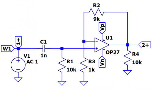
Now consider the next circuit in figure 8.

Figure 8. Active High Pass Filter with Gain Control circuit
The filter circuit is an Active High Pass Filter which basically passes and amplifies high frequency. The circuit is composed of RC high pass filter providing a high-frequency pass with the addition of the op-amp for gain control and amplification. The frequency response of the filter is the same compared to a passive high pass filter. The gain, A, of the output signal is dependent on the input resistor (R3) and feedback resistor (R2), the same as that in non-inverting active low pass filter.
The gain of the first-order high pass filter as a function of frequency will be:
Where:
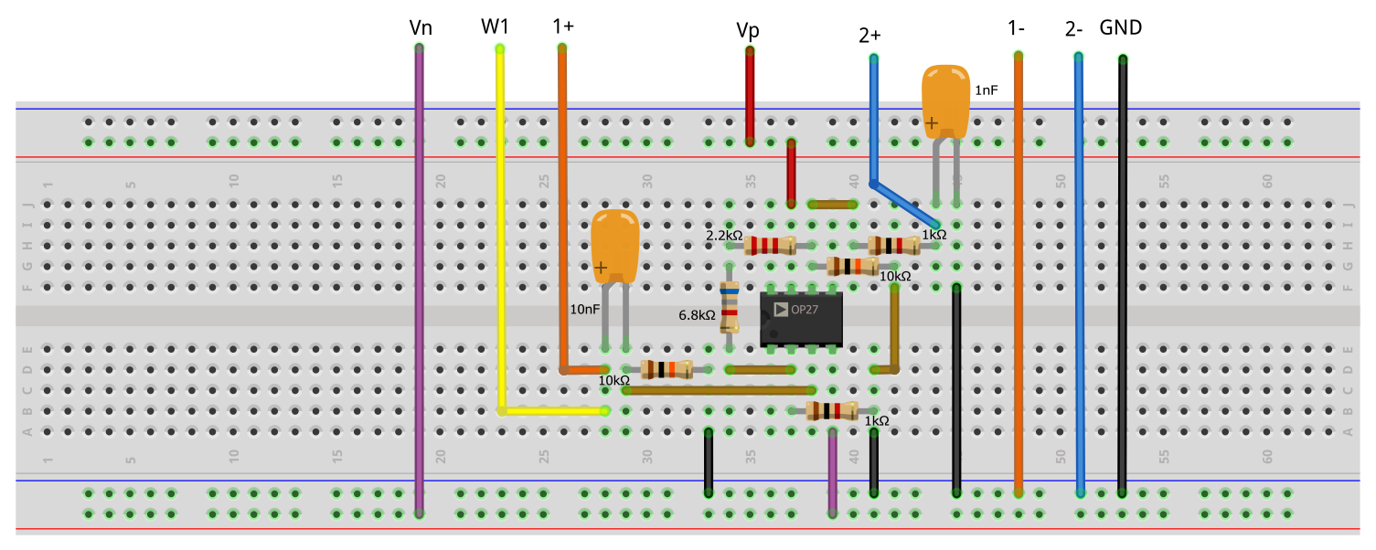
Construct the active high pass filter circuit shown in figure 8. Use the positive and negative positive supply from the ADALM2000.

Figure 9. Active High Pass Filter with Gain Control circuit
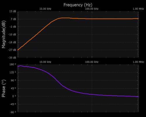
On Scopy Network Analyzer, set Channel 1 as the reference. Set the Amplitude to 200mV, 0V offset. Under the display settings, set the max. magnitude to 30 dB and min. magnitude to –25 dB. Set phase from -180 º to +180 º. Set sample count to 100.
Turn on the power supplies and run a single frequency sweep from 500Hz to 1MHz.

Figure 10. Active High Pass Filter with Gain Control circuit
Comparing the result to an ideal frequency response of a passive high pass filter, the frequency response of an active high pass filter is limited to the op-amp’s bandwidth or open loop characteristics. There comes a point on the spectrum that the gain decreases as the frequency increases making the whole response look like a bandpass filter.
Unlike the previous filter configurations shown above in which the pass band is determined only by one cut-off frequency, DC up to the cut-off frequency for the low pass filter and cut-off frequency onward for the high pass filter, the active band pass filter has two cut-off frequencies that define the selected frequency range. A simple configuration of the active band pass filter is shown in figure 11.
Figure 11. Active Band Pass Filter
The circuit is composed of 3 stages. The first stage is the RC high pass filter which defines the lower cut-off frequency, fL, and attenuates signals below this defined frequency. Then the next stage is the Amplification Stage which basically is the op-amp amplifying the signals passed by the high pass filter stage. And lastly, the RC low pass filter stage which defines the higher cut-off frequency, fH, and attenuates signals falling above this defined frequency. The difference between the higher cut-off frequency and lower cut-off frequency determines the bandwidth of the band pass filter.
The voltage gain of this filter is given by the expression,
Where:
Taking a closer look at the circuit, the presented active band pass filter is basically a second order system. By cascading one low pass filter and one high pass filter gives us a second-order band pass filter. Having two reactive components, capacitors, the filter will have a peak response, Resonant Frequency, fr, which is the geometric mean of the two cut-off frequencies. The resonant frequency is also called the Center frequency, but in this activity let's use the term resonant frequency.
Aside from the cut-off frequencies defining the resonant frequency, it also determines the quality factor of the filter. This Quality Factor, Q, is a measure of selectivity of the filter and is defined as the quotient of the resonant frequency with regards to the bandwidth. The Q factor, along with the gain and resonant frequency characterizes the frequency response of the second order filter.
When Q is greater than 1, the band-pass filter has a much narrower pass band whereas when Q is lesser than 1, a wider pass band.
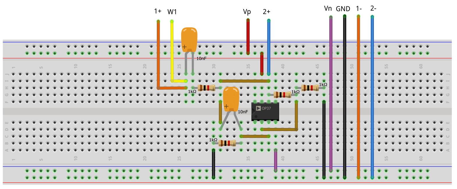
Build the breadboard circuit presented in figure 12. Use the positive and negative power supply from the ADALM2000.

Figure 12. Active Band Pass Filter breadboard connection
On Scopy Network Analyzer, set Channel 1 as the reference. Set the Amplitude to 200 mV, 0 V offset. Under display settings, set magnitude from -10 dB to 25 dB and phase from -150º to 100º. Set sample count to 100.
Turn on the power supplies and run a frequency sweep from 100Hz to 500kHz.

Figure 13. Active High Pass Filter Frequency Response
Another type of filter can be made from combining a low pass filter and a high pass filter. Such filter configuration is a Band Stop Filter.
Figure 14. Active Band Stop Filter circuit
The filter circuit shown in Figure 14 is an Active Band Stop or Active Band reject Filter circuit. It operates exactly the opposite of the Active Band pass Filter. This filter blocks and attenuates the frequencies between the lower and higher cut-off frequencies but passes signals from DC to the lower cut-off frequency and all the frequencies above the higher cut-off frequency.
The circuit is composed of a combined high pass and low pass filters. The input signal is simultaneously fed to both the inputs of the high pass and low pass filters. The output of each filter then becomes the input to the summing amplifier and are amplified. By summing the low pass and the high pass filters, their frequency responses do not overlap. Similarly, like the band-pass filter, the band stop filter is a second order system.
Bandstop filter's definition for bandwidth, quality factor, and the resonant frequency is the same as the band-pass filter.
Like the band-pass filter, the band stop filter has a wider stop band when Q is less than 1 and a much narrower stop band when Q is greater than 1. A narrow-band band stop filter is referred to as a Notch Filter. The band stop filter in Figure 14 is an example of a notch filter.
On your breadboard, build the circuit shown in Figure 15. Set +5V for the positive supply and -5V for the negative supply.
Figure 15. Active Band Stop Filter Circuit breadboard connection
On the Network Analyzer instrument, set Channel 1 as a reference and set the sweep logarithmic from 10Hz to 500 kHz with a sample count of 250. Under the waveform settings, set the amplitude to 200 mV and 0 V offset. Set the display from -30 dB to 30 dB and -180º to +180º. Turn on the power supplies and observe the waveform.
Figure 16. Active Band Stop Filter Circuit Frequency Response
Given the previous circuits above, you might have observed the difference between the active low/high pass filters to the active band pass/band stop filters. What makes the band pass and band stop filter a second order filter system? Second Order Filters would have two reactive components in the circuit which affects the frequency response of the filter. Added reactive components to the circuit configuration, such as cascading two first order filter, would double the gain roll-off rate to -40dB/roll-off.
Second Order Filters are another important type of active filter design because along with the active first order RC filters, they are used as building blocks to design higher order filter circuits. Second Order Filters are also referred to as VCVS filters because the op-amp is used as a Voltage Controlled Voltage Source amplifier.
There are plenty of second order filter configurations available such as Butterworth, Chebyshev, Bessel, and Sallen-Key. The Sallen-Key filter design is one of the most popular second order filter design because of its simplicity. It requires only four passive RC components for frequency tuning and a single op-amp for the gain control.
Figure 17. Sallen Key Second Order Low Pass Filter
Shown in Figure 17 is the basic configuration of a Sallen Key second order low pass filter. The filter circuit has two RC networks which give the filter the frequency response properties. R1-C1 and R2-C2 networks define the cut-off frequency of the filter which can be computed with the following equation,
The gain of the amplifier, A, is of a non-inverting amplifier. Thus, we make use of the formula we had used earlier,
One other concept we’ve encountered earlier is the quality factor, just like the band pass and band stop filter which are second-order systems. The Sallen Key quality factor can be computed with the following equation,
The value of Q can also be related to the dampness of the system. The relationship of dampness to Q can be summarized to the following conditions,
The relationship between Q and A is critical in Sallen Key configuration which makes it its limitation. Q must be greater than ½ since A must be greater than 1.
Build the breadboard circuit presented in Figure 18. Use the positive and negative power supply from the ADALM2000.

Figure 18. Sallen Key Second Order Low Pass Filter breadboard connection
Set Channel 1 as the reference. Set the Amplitude to 200 mV, 0 V offset. Under display settings, set magnitude from -20 dB to 15 dB and phase from -270º to 90º. Set sample count to 100.
Turn on the power supplies and run a frequency sweep from 100Hz to 500kHz.

Figure 19. Sallen Key Second Order Low Pass Filter Frequency Response
Now consider the Sallen Key configuration of a high pass filter presented in Figure 20.

Figure 20. Sallen Key Second Order High Pass Filter
The configuration is like the low pass configuration except that the positions of the resistors and capacitors are interchanged. 2nd order Sallen-Key filters are also referred to as positive feedback filters since the output feeds back into the positive terminal of the op-amp.
Build the breadboard circuit presented in Figure 21. Use the positive and negative power supply from the ADALM2000.

Figure 21. Sallen Key Second Order High Pass Filter breadboard connection
Set Channel 1 as the reference. Set the Amplitude to 200 mV, 0 V offset. Under display settings, set magnitude from -35 dB to 15 dB and phase from -90º to 180º. Set sample count to 100.
Turn on the power supplies and run a frequency sweep from 7.5kHz to 1MHz.

Figure 22. Sallen Key Second Order High Pass Filter Frequency Response
The band-pass configuration of the Sallen-Key filter has a severe limitation. The Q value determines the gain of the filter, that is, it cannot be set independently, as it can with the low pass or high-pass cases. The voltage gain can be computed using the following equation,
Figure 23. Sallen Key Second Order Band pass Filter
Shown in Figure 23 is the Sallen Key second-order band pass filter configuration.
Build the breadboard circuit presented in Figure 24. Use the positive and negative power supply from the ADALM2000.

Figure 24. Sallen Key Second Order Band pass Filter breadboard connection
Set Channel 1 as the reference. Set the Amplitude to 200 mV, 0 V offset. Under display settings, set magnitude from -35 dB to 5 dB and phase from -180º to 180º. Set sample count to 100.
Turn on the power supplies and run a frequency sweep from 7.5kHz to 1MHz.

Figure 25. Sallen Key Second Order Bandpass Filter Frequency Response
It is also possible to design Sallen Key notch filter but it has undesirable characteristics. The resonant frequency, or the notch frequency, cannot be adjusted easily due to component interaction. Thus, it is not included in this lab activity. Although you can try simulating the Sallen Key notch filter circuit in LTSpice, the schematic can be found on the link at the bottom of this page.
State Variable Filter configuration offers the most precise implementation of the filter function, at the expense of many more circuit elements. All three major parameters (gain, Q, and fr) can be adjusted independently, and low-pass, high-pass, and band-pass outputs are available simultaneously. A notch and all pass filter are also possible to configure using the state variable filter. With an added amplifier section summing the low-pass and high-pass sections, the notch function can also be synthesized. An all pass filter may also be built with the four-amplifier configuration by subtracting the band-pass output from the input. Shown in Figure 26 is the state variable filter configuration that output and low-pass, high-pass, and band-pass frequency response.

Figure 26. State Variable Filter
Tuning the resonant frequency of a state variable filter is accomplished by varying R4 and R5. While you do not have to tune both, it is generally preferable if you are varying over a wide range. Holding R1 constant, tuning R7 sets the low-pass gain and tuning R2 sets the high-pass gain. Band-pass gain and Q are set by the ratio of R3 and R7. Note that the low-pass and high-pass outputs are inverted in phase while the band-pass output maintains the phase.
Build the breadboard circuit presented in Figure 27.

Figure 27. State Variable Filter breadboard connection
Connect Channel 2 to the Low Pass filter output.
Set Channel 1 as the reference. Set the Amplitude to 200 mV, 0 V offset. Under display settings, set magnitude from -40 dB to 30 dB and phase from -45º to 180º. Set sample count to 100.
Turn on the power supplies and run a frequency sweep from 100Hz to 250kHz.

Figure 28. State Variable Filter, Low Pass Frequency Response
Now, try connecting channel 2 to either band pass or low pass output and run a sweep.
Another example of a Second Order Active Filter is the Tow-Thomas Filter, sometimes referred to as Biquadratic (Biquad) Filter. Figure 29 shows an example of the Tow-Thomas (Biquad) Filter.
Figure 29. Tow-Thomas Filter circuit
The Tow-Thomas Filter is tunable like the state variable (KHN) filter: Adjust R3 to change the Q-factor, R4 to change the resonant frequency, and R1 to set the gain. To minimize the effects of component value interaction, adjust the resonant frequency first followed by the Q and finally the gain. The bandwidth of the Tow-Thomas filter is defined as:
Upon closer look, the Tow-Thomas Filter configuration is a minor rearrangement of the state variable filter. It has no separate high-pass output, but it generates two low-pass outputs, one in phase and the out of phase, and a band-pass output that inverts the phase. Connections of each output are seen in Figure 29. However, adding a fourth amplifier to the current filter configuration allows the filter to generate either high-pass, notch, or all-pass filters. An all-pass filter adds a phase shift response to the circuit while leaving the amplitude of the signal untouched. It has a unity gain for all frequencies.
Build the breadboard circuit presented in Figure 30 on your breadboard. Set the positive supply to +5 V and the negative supply to -5 V.
Figure 30. Tow-Thomas Filter Circuit breadboard connection
Set sweep as logarithmic with Channel 1 as the reference, the amplitude to 200 mV with 0 V offset, and the samples count to 75. Set the display from -60 dB to 30 dB and from -30º to 210º. Turn on the power supplies and run a single frequency sweep from 100 Hz to 500 kHz.
Figure 31. Tow-Thomas Filter Circuit Frequency Response
The circuit shown in Figure 32 is a Twin-T Notch Filter. It is used as a general-purpose notch (narrow band stop) circuit. Recall that a band stop filter attenuates and blocks frequencies between its lower and higher cut-off frequencies.
Figure 32. Twin-T Notch Filter circuit
The Twin-T Notch filter circuit is composed of two T-shaped networks: An RCR T-network and a CRC T-network. Resistors R1 and R2 with capacitor C3 form the RCR T-network while capacitors C1 and C2 alongside with resistor R3 form the CRC T-network. The design configurations are shown below:
Take note of the values of R and C. These two determines the center notch frequency fo of the filter which is defined by the expression:
In its passive implementation, the Twin-T notch filter has its Q fixed at 0.25. Implementing positive feedback to the reference node can fix the problem. This is done by setting up a voltage divider using R4 and R5 at the output of the filter and connect it to a voltage follower. Then, the output of the voltage follower is supplied back to the junction of R3 and C3.
The signal feedback is given by the resistors R4 and R5 determine the Q of the filter as well as the notch depth. The quality factor is defined as:
To achieve the maximum notch depth, eliminate resistors R4 and R5 alongside the op-amp connected to them and connect the junction between R3 and C3 junction directly to the output.
On your breadboard, build the circuit in Figure 33. Use the positive and negative supplies of the ADALM2000. Figure 34 replaces R4 and R5 with a potentiometer allowing more control for the Q of the circuit.
Figure 33. Twin-T Notch Filter Circuit breadboard connection
Figure 34. Twin-T Notch Filter Circuit with Potentiometer breadboard connection
Set sweep as logarithmic with Channel 1 as the reference, the amplitude to 200 mV with 0 V offset, and the samples count to 100. Set the display from -25 dB to 5 dB and -140º to 80º. Turn on the +5 V and -5 V power supplies and sweep from 30 kHz to 300 kHz.
Figure 35. Twin-T Notch Filter Circuit Frequency Response
Your circuit’s frequency response should be similar to your simulation result.
1. Considering the circuit in Figure 17, change the gain of the amplifier by replacing values of R3 and R4. What do you observe with the frequency response? Do the same in Figure 20 and 23.
Lab Resources: