A variety of digital logic circuit techniques have been in use since the 1960s, when integrated logic gates were first produced. In this Lab activity, the Transistor Transistor Logic (TTL) circuit inverter (NOT gate) and 2 input NAND gate configurations are examined.
The schematic of a Transistor Transistor Logic (TTL) inverter is shown in figure 1. This circuit overcomes the limitations of the single transistor inverter circuit. The basic TTL inverter consists of three stages. A current steering input, a phase splitting stage and an output driver stage.
Figure 1 TTL Inverter
The input stage transistor Q1 performs a current steering function. It can be thought of as a back-to-back diode arrangement. The transistor is operated in either forward or reverse mode to steer current to or from the second stage transistor's base, Q2. The forward current gain or ßF, is much larger than the reverse ßR. it provides a higher discharge current to discharge the base when turning it off.
Figure 2 Equivalent circuit of input current steering stage
Second stage transistor, Q2 in figure 1, is a phase splitter transistor to drive both halves of the pull up and pull down output stage. It allows the input condition to be produced in opposite phases so that the output transistors can be driven in anti-phase. This allows Q3 to be on when Q4 is off and vice versa as shown in figure 3.
Figure 3 Phase splitting stage
The output transistor pair, Q3 and Q4 along with diode D1 are referred to as a totem-pole output as shown in figure 4. This output configuration provides the ability to both actively source or sink current and is useful for driving capacitive loads. Resistor R4, serves to limit the current available from VCC. Under steady-state conditions, only one transistor is on at a time.
Figure 4 Output Stage
The diode, D1, serves to increase the effective turn on voltage of Q4 which allows it to be turned off before Q3turns fully on. This helps prevent potentially large surge currents from flowing in the output stage during transitions between logic states. Resistor R4 also serves to limit the current that is allowed to flow in the output stage. The disadvantage is that the logic high voltage is reduced by an amount of the diode drop as shown in figure 7.
ADALM2000 Active Learning Module
Solder-less breadboard
Jumper wires
1 - 100 KΩ Resistor
1 - 2.2 KΩ Resistor
1 - 470 Ω Resistor
1 - 100 Ω Resistor
1 - small signal diode (1N914)
5 - small signal NPN transistors (2N3904)
Build the circuit shown in figure 5 on your solder-less bread board. The NPN transistors supplied with your ADALP2000 Parts Kit are limited to 5 2N3904 and 1 TIP31 power transistor. Use the 5 2N3904 transistors and a 1N914 diode. First, connect the TTL inverter circuit on your breadboard.
Figure 5 TTL Inverter
Connect your circuit to the ADALM2000 I/O connector as indicated by the green boxes. It is best to ground the unused negative scope inputs when not being used. The breadboard connections are shown in figure below.

Figure 6 TTL Inverter Breadboard Circuit
Configure waveform generators, W1, with 100 Hz triangle wave with 0 V offset and 6 V amplitude peak-to-peak peak-to-peak values. Use the oscilloscope in the x-y mode to observe the voltage-transfer curve of the circuit.

Figure 7 TTL inverter transfer curve
By adding another input to the TTL inverter, a TTL NAND gate can be made. Connect the TTL inverter circuit, shown on figure 8.

Figure 8 TTL two input NAND Gate
Connect your circuit to the ADALM2000 I/O connector as indicated by the green boxes. It is best to ground the unused negative scope inputs when not being used. The breadboard connections are shown in figure below.

Figure 9 TTL two input NAND Gate Breadboard Circuit
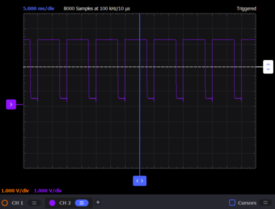
Configure waveform generators, W1, with 100 Hz triangle wave with 0 V offset and 6 V amplitude peak-to-peak values and W2, 100 Hz triangle wave with 0 V offset and 6 V amplitude peak-to-peak values and 90° phase. Use the oscilloscope to observe the output of the circuit, CH2.

Figure 10 TTL NAND Gate Output Waveform
The output circuitry of a typical TTL logic gate is commonly referred to a totem-pole output because the two output transistors are stacked one above the other like carvings on a totem pole. Is a gate circuit with a totem-pole output stage able to source load current, sink load current, or do both?
*Resources:*
http://en.wikipedia.org/wiki/Transistor-transistor_logic
Return to Lab Activity Table of Contents