To investigate a simple push-pull amplifier output stages (class B and AB).
The role of an output stage is to provide power gain. It should have high input impedance and low output impedance. An obvious choice for this stage is the emitter follower. However, in order to provide both current sourcing and sinking capabilities, two complementary followers are needed, an NPN type to source and a PNP type to sink current. The result is known as the push-pull configuration, of which figure 1 shows a simple configuration. Here R1 and R2 are used to sense the collector currents of Q1 and Q2, as well as to limit these currents in case of output overloading.
ADALM2000 Active Learning Module
Solder-less breadboard
Jumper wires
2 - 100 Ω resistors
1 - 2.2 KΩ resistor
2 - 10 KΩ resistors
2 - small signal NPN transistors (SSM2212 with matching VBE preferred)
2 - small signal PNP transistors (SSM2220 with matching VBE preferred)
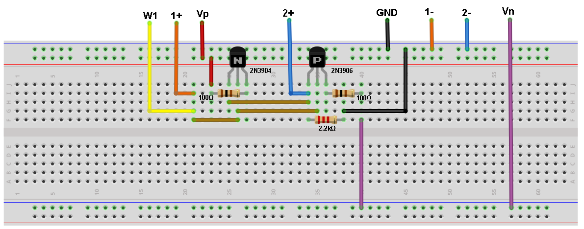
Before starting make sure the power supplies on the ADALM2000 are turned off. The circuit and the connections to the Lab hardware are as indicated in figure 1. Scope input 1+ should to be connected to the junction of Q1 and Q2 bases. Scope input 2+ should to be connected to the junction of Q1 and Q2 emitters.
Figure 1 Push - Pull Output stage
Channel one of the scope should be connected to display the output of the first generator and both scope channels 1 and 2 should be set to display 1V per division. The breadboard connections are shown in figure 2.

Figure 2 Push - Pull Output stage Breadboard Circuit
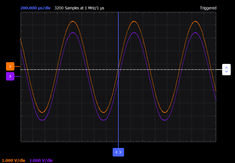
The waveform generator, W1, should be configured for a 1 KHz sine wave with 6.0 volt amplitude peak-to-peak and 0 offset. Using scope channel 1 to observe the input at W1 and scope channel 2 to observe the output of the amplifier at RL.

Figure 3 Push - Pull Output stage Waveforms
Next, apply power and adjust the waveform generator so that W1 is a 100 Hz triangle wave with 0V offset and 3.0 V amplitude peak-to-peak. Use the oscilloscope in the x-y mode to observe the voltage-transfer curve of the circuit.
Figure 4 Voltage-transfer curve
Record the curve on paper, label all breakpoints, slopes, and saturation levels, and justify them in terms of circuit operation and given component values.
Switch the scope to just the time display mode, and adjust the waveform generator so that W1 is a 1 kHz sine wave with the amplitude = 0 V.
• Starting with the amplitude = 0 V, gradually increase it until you just begin to see a signal on scope channel 2 appear at the output. For what range of amplitude values of W1 can we say that both BJT's are essentially off? Confirm this by observing the voltages of the current-sensing resistances R1 and R2.
• Raise W1 to 6.0V amplitude peak-to-peak value, and record the amplitude of the output waveform as well as the collector currents of the BJTs, which can be found via Ohm's law from the voltages across R1 and R2, and justify your findings in terms of circuit operation and the given component values.
• Repeat, but with W1 raised a 10.0V amplitude peak-to-peak value; and comment.
Simulate the circuit of figure 1 using QUCS, compare with your lab findings, and justify any differences.
The large amount of distortion at the zero-crossings in the basic push-pull stage of figure 1 is a result of a dead zone when both the NPN and PNP emitter followers are off. The waveform's dead zone at the zero-crossings is dramatically reduced if we pre-bias the BJTs with two VBE drops, as shown in figure 2. Here, the pre-bias function is provided by diode connected NPN Q1 and PNP Q3. Resistors R1 and R2 provide bias current and set the idle current that flows in the output devices Q2 and Q4.
With the power turned off, assemble the circuit of figure 5, keeping leads as short and neat as possible. NPN transistors Q1 and Q2, PNP transistor Q3and Q4 should be selected from the available devices with the best matching of VBE. Transistors fabricated in the same package such as the SSM2212 or the CA3046 tend to match much better than individual devices.
Figure 5 Push - Pull output stage with zero-crossing distortion elimination.
If we examine, in figure 5, the loop formed by the base emitter voltages of Q1, Q2, Q3 and Q4 we know that the sum of the voltage drops around the loop must sum to zero. Thus if Q1 is identical to Q2 and Q3 is identical to Q4, the voltage around the loop will be zero only when the current in Q1 is identical to the current in Q2 and the current in Q3 is identical to the current in Q4. Thus when the output is at zero volts i.e. there is no current in RL, the input must also be at zero volts.
Channel one of the scope should be connected to display the output of the first generator and both scope channels 1 and 2 should be set to display 1V per division. The breadboard connections are shown in figure 6.

Figure 6 Push - Pull Output stage with zero-crossing distortion elimination Breadboard Circuit
The waveform generator, W1, should be configured for a 1 KHz sine wave with 6.0 volt amplitude peak-to-peak and 0 offset. Using scope channel 1 to observe the input at W1 and scope channel 2 to observe the output of the amplifier at RL.

Figure 7 Push - Pull Output stage with zero-crossing distortion elimination Waveforms
• Display the input / output transfer curve of the circuit of figure 5, record it on paper, label all breakpoints, slopes, and saturation levels, and justify them in terms of circuit operation and the given component values.
• Apply a 1-kHz sine wave of 0 V offset and various amplitudes, and verify that the circuit yields Vout ? Vin all the way down to small amplitudes. What is the upper limit on the amplitude of W1 before the circuit starts to distort? Justify quantitatively in terms of the transfer curve just observed.
Using your scope input, measure Vout as well as the voltage across R3 and R4 for the following DC values of Vin: -5 V, -4 V, -3 V, … 0 V, … , +4 V, +5 V. Then, tabulate Vout and the current in RL as well as the collector currents of Q2 and Q4 and comment. Use the offset of the waveform generator to set the DC value with the amplitude set to 0V.
Measure the input impedance by inserting a 10K? resistor in series with the signal generator (between W1 and the emitters of Q1and Q3) and connecting the channel 1 differential scope inputs, 1+ , 1- across the 10K? resistor. Capture the input current vs. the input voltage and calculate the input resistance from the slope of the curve. Justify your results based on the component values used in the circuit.
Simulate the circuit of figure 5 using QUCS, compare with your lab findings, and justify any differences.
Remembering the loop formed by the base emitter voltages of Q1, Q2, Q3 and Q4 we also know that the order of the voltage drops around the loop can be interchanged. So if we interchange the VBE's of NPN Q1 and PNP Q3 we get the configuration shown in figure 3. Some of you may recognize the combination of Q3 and Q2 as the low offset follower we discussed earlier in the lab section on emitter followers. The circuit uses the VBE shift up of a PNP emitter follower to partially cancel the VBE shift down of an NPN emitter follower. Transistors Q1 and Q4are simply the complement of Q3 and Q2.
Figure 8 Emitter Follower zero-crossing distortion elimination
Channel one of the scope should be connected to display the output of the first generator and both scope channels 1 and 2 should be set to display 1V per division. The breadboard connections are shown in figure 9.

Figure 9 Emitter Follower zero-crossing distortion elimination Breadboard Circuit
The waveform generator, W1, should be configured for a 1 KHz sine wave with 6.0 volt amplitude peak-to-peak and 0 offset. Using scope channel 1 to observe the input at W1 and scope channel 2 to observe the output of the amplifier at RL.

Figure 10 Emitter Follower zero-crossing distortion elimination Waveforms
Lab Resources:
• Display the input / output transfer curve of the circuit of figure 3, record it on paper, label all breakpoints, slopes, and saturation levels, and justify them in terms of circuit operation and the given component values. How do they compare to the circuit in figure 2?
• Apply a 1 kHz sine wave of 0 V offset and various amplitudes, and verify that the circuit yields Vout ? Vin all the way down to small amplitudes. What is the upper limit on the amplitude of W1 before the circuit starts to distort? Justify quantitatively in terms of the transfer curve just observed.
Using your scope input, measure Vout as well as the voltage across R3 and R4 for the following DC values of Vin: -5 V, -4 V, -3 V, … 0 V, … , +4 V, +5 V. Then, tabulate Vout and the current in RL as well as the collector currents of Q2 and Q4 and comment. Use the offset of the waveform generator to set the DC value with the amplitude set to 0V.
Measure the input impedance by inserting a 10KΩ resistor in series with the signal generator (between W1 and the bases of Q1and Q3) and connecting the channel 1 differential scope inputs, 1+ , 1- across the 10KΩ resistor. Capture the input current vs. the input voltage and calculate the input resistance from the slope of the curve. Justify your results based on the component values used in the circuit. How do your results compare to what you measured for the circuit in figure 5?
Simulate the circuit of figure 3 using LTSpice or ADIsimPE, compare with your lab findings, and justify any differences.
Resources:
Output Stages (MT-207)
Push-Pull Outputs
Return to Lab Activity Table of Contents