


This version (30 Jan 2023 18:17) was approved by Iulia Moldovan.The Previously approved version (30 Jan 2023 09:21) is available.
Table of Contents
AD9783 Evaluation Board, DAC-FMC Interposer & Xilinx Reference Design
The AD9783 includes pin-compatible, high dynamic range, dual digital-to-analog converters (DACs) with 16-bit resolution, and sample rate of up to 500 MSPS.
The device includes specific features for direct conversion transmit applications, including gain and offset compensation, interfacing seamlessly with analog quadrature modulators.
Supported Devices
Supported Carriers
Functional Description
Block Diagram
The reference design consists of a DDS module and a LVDS interface.
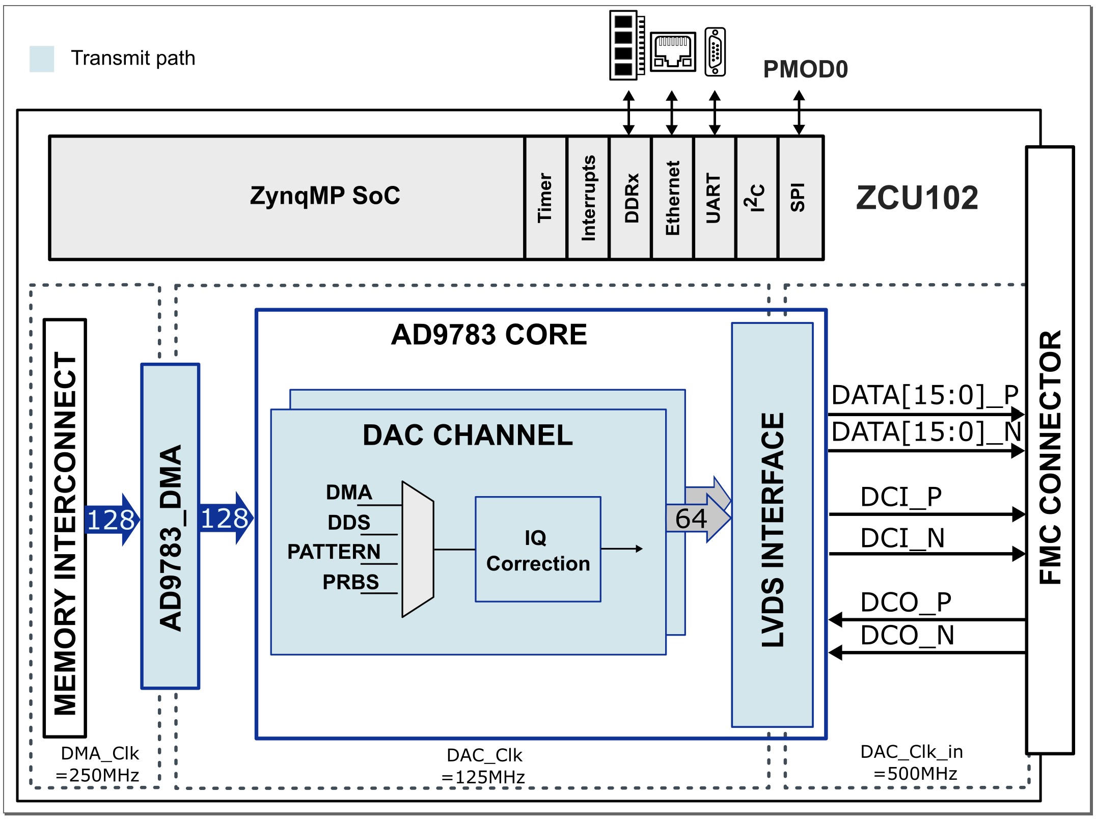
Description
Creating the constraints
When creating the constraints file for this project, the AD9783-EBZ, AD-DAC-FMC-ADP and ZCU102 schematics were used, because we have to make a correspondence between the signals from one side and the other.
First, we look in the AD9783-EBZ schematic and we spot the signals we have to use in the HDL design, like D[15:0] LVDS pairs, DCI_P and _N, DCO_P and _N, and the SPI signals (SDIO, SDO, SCLK and CSB).
Then, we check which pins are their correspondents in the AD-DAC-FMC-ADP schematic.
Example:
AD9783-EBZ schematic: D15P is connected to J17 plug header, at A3
AD-DAC-FMC-ADP schematic: J17 plug header pin A3 is called TXI_DATA_P15 and is connected to CLK1_M2C_P pin from P1 FMC header
ZCU102 schematic: pin CLK1_M2C_P is pin T8 in FMC HP0
Thus we have this constraint:
set_property -dict {PACKAGE_PIN T8 IOSTANDARD LVDS} [get_ports data_p[15]] ; ## G2 FMC_HPC0_CLK1_M2C_P
Quick Start Guide
Required Hardware
- ZCU102 board
- AD9783-EBZ board & power supply
- Signal/clock generator (2.5GHz)
- Spectrum analyzer
- 5Vdc 1A power supply (banana cables) for the evaluation board
- 1x USB Mini-B to connect to the evaluation board
- 1x USB Micro-B to connect to UART
- 2x SMA cables
Required Software
- An UART terminal, with baud rate 115200
Setup
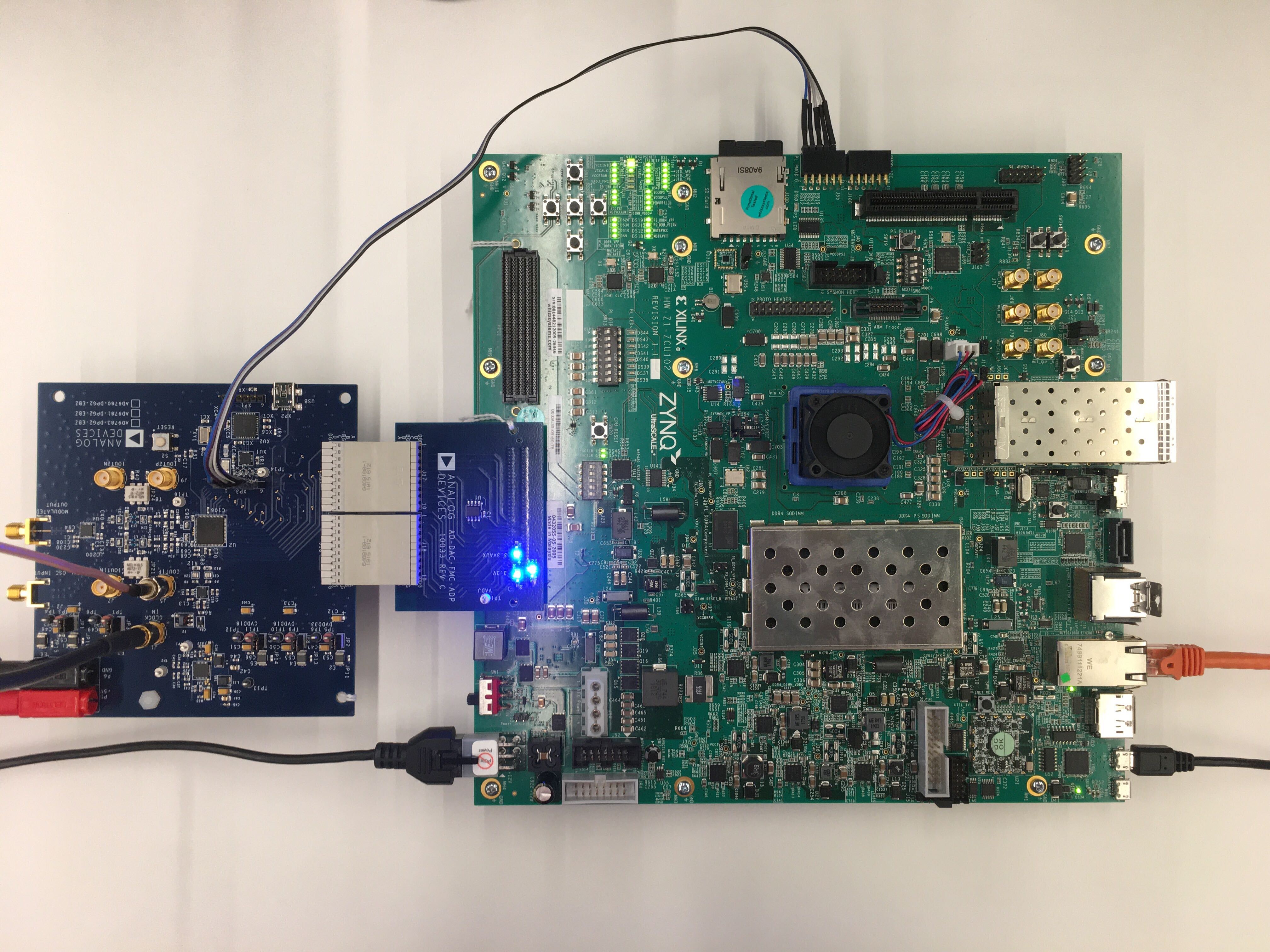
- Hardware adjustments:
- Desolder XJP1, 3, 4, 5 from AD9783-DPG-EBZ in order to use the SPI communication through the cable from step 3 and directly into the ZCU102's PMOD0
- Check that the desoldering was done properly and there is no current from one side to the other
- Attach AD9783-DPG2-EBZ to ZCU102 FMC 0 connector using the AD-DAC-FMC-ADP adapter board
- Connect a 5 wire cable from AD9783-EBZ's XP3 to ZCU102's PMOD0 (see pinout from the photo below):

- Prepare the SD card:
- Prepare the latest Linux image from SDCARD for Zynq & Altera SoC Quick Start Guide wiki page. Follow those steps and then continue from here.
- From zynqmp-common folder of the boot partition, copy the Image file into the root folder of the partition
- From zynqmp-zcu102-rev10-ad9783 folder of the boot partition, copy the system.dtb and BOOT.BIN files into the root folder of the partition
- Insert the SD card into the ZCU102 SD card slot
- Connect clock source for the clock input at J1 on the evaluation board via a SMA cable, and DAC output at J5 (IOUT1P) or J9 (IOUT2P) via a SMA cable to a spectrum analyzer
- Connect the UART port on ZCU102 via USB Micro-B to PC
- Set the clock input to 500MHz, +3dBm
- Connect the evaluation board to a 5Vdc 1A power supply on P5 and P6
- Power on the evaluation board, clock generator and ZCU102
- Write the EEPROM found on the AD-DAC-FMC-ADP to set the Vadj to 1.8V, using the tutorial FRU EEPROM Utility. The file you will write on the EEPROM, can be found on the fru_tools repository: download the AD9783-DPG2-EBZ.bin file from masterfiles folder onto your SD card.
Troubleshooting
- Check if the voltage supply test points of the evaluation board has the correct value
- Check if all (3) blue LEDs on the AD-DAC-FMC-ADP board are lit up. Reconnect the board to the FMC connector of the carrier if not lit up
- Check if the carrier is being supplied properly
- Check on the Spectrum Analyzer if the DAC clock inputs are properly driven. If not detected, check properly the clock source and connections.
resources/fpga/xilinx/interposer/ad9783.txt · Last modified: 30 Jan 2023 18:17 by Iulia Moldovan