


This version (14 Feb 2021 22:29) was approved by Dragos Bogdan.The Previously approved version (09 Jan 2021 00:39) is available.
Table of Contents
AD9739A Native FMC Card / Xilinx Reference Designs
Introduction
The AD9739A is a 14-bit, 2.5 GSPS high performance RF DAC capable of synthesizing wideband signals with up to 1.25GHz of bandwidth. This reference design includes a single tone sine generator (DDS) and allows programming the device and monitoring its internal status registers. It also programs the ADF4350 clock chip which can generate a 1.6GHz to 2.5GHz clock for the AD9739A from the on-board 25MHz crystal. An alternate clock path using an ADCLK914 is available for driving the clock externally.
Supported Devices

The AD9739A FMC Card is not fully ANSI/VITA 57.1 compatible:
- does not meet the mechanical form factor (too tall, too long),
- does not include the I2C EEPROM as specified in Rule 5.69,
- Also see “bugs” below.
It was designed, and meets the needs of prototyping platforms, and will work with FPGA Development systems which include an FMC connector. It may not mechanically fit on other ANSI/VITA 57.1 carrier cards.
Supported Carriers
Quick Start Guide
The reference design has been tested on ML605(Virtex-6), KC705(Kintex-7), VC707(Virtex-7) and ZC706 (Zynq) boards. The notes below refer to ML605, however the procedure is same for the other boards. Currently, we fully support only the ZC706 Vivado based design. Please make sure that you have downloaded and are using the correct design files for your board. All you need is the hardware and a PC running a UART terminal.
A video tutorial is available: 1423927819001
Required Hardware
- ML605/KC705/VC707/AC701 board (use the corresponding design file).
- AD9739A-FMC-EBZ board
- Spectrum Analyzer
Required Software
- Xilinx ISE Design Suite 14.4
- A UART terminal (Tera Term/Hyperterminal), Baud rate 57600.
Running Demo (SDK) Program
To begin, connect the AD9739A-FMC-EBZ board to the FMC-LPC connector of ML605 board (see image below). If using KC705 use FMC-LPC, if using VC707 use FMC1-HPC. Connect power and two USB cables from the PC to the JTAG and UART USB connectors on the edge of the ML605. A spectrum analyzer should be connected to the output SMA jack (OUT/J1). This quick start program uses a 2.5GHz DAC clock and generates a 300MHz tone. Adjust your spectrum analyzer accordingly. On the AD9739A-FMC board, ensure that the SPI source jumper (SPI SRC/P2) is set to FMC and the clock source jumper (CLOCK SOURCE/S1) is set to ADF4350 position. The USB connection on the AD9739A-FMC-EBZ and the SMA Clock Input (SMA CLKIN/J3) are not used in this example. After the hardware setup, turn the power on to the ML605.

Run the download.bat script located in the “SDK/SDK_Workspace/bin” folder provided within the HDL Reference Design. This script uses XMD to program the FPGA with the HDL Reference Design and download the Software Reference Design into the DDR.
Note: The download.bat script assumes that the Xilinx ISE Design Suite 14.4 is installed at this path: C:/Xilinx/14.4. If the installation path on your computer is different please modify the script accordingly.
If programming was successful, you should be seeing messages appear on the terminal as shown in figure below. After programming the AD9739A and ADF4350, you have to tell the program from where it should take the input data(from DMA or DDS). Then the program continuously monitors the MU Controller and LVDS Receiver lock status. If either of them are out of lock, the program quits itself with an error. You may also quit the program by pressing [q] key.

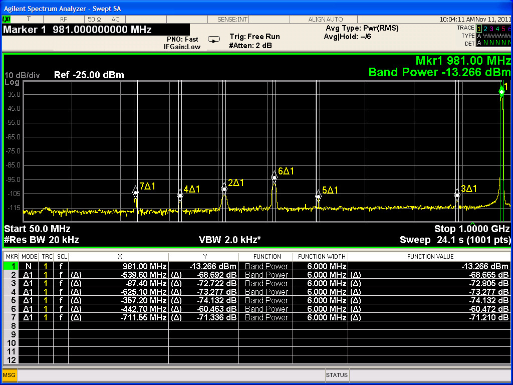
The specturm analyzer output is shown below.

DOCSIS Results
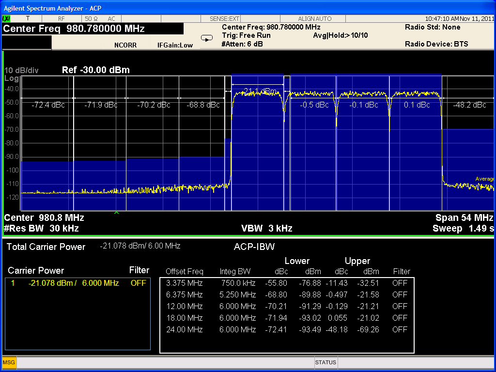
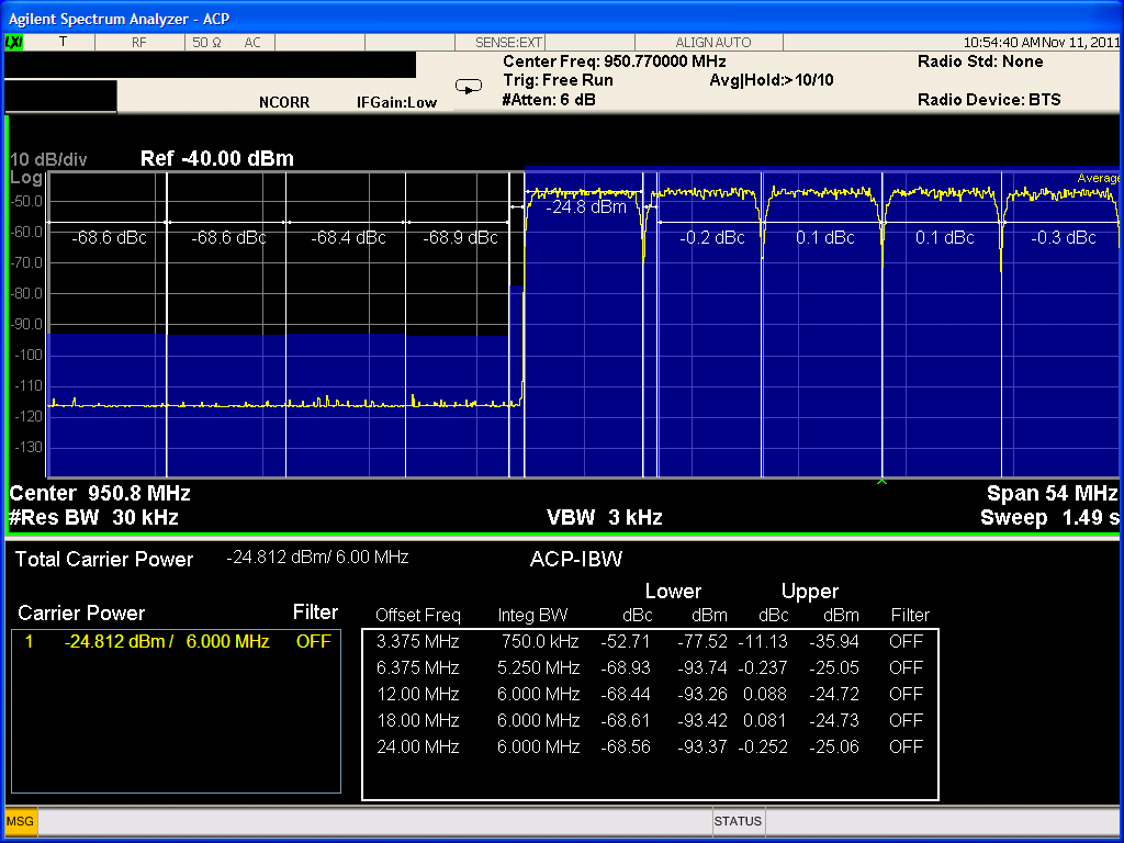
Data Over Cable Service Interface Specification is an international telecommunications standard that permits the addition of high-speed data transfer to an existing cable TV (CATV) system. It is employed by many cable television operators to provide data access over their existing infrastructure. It has many specification, certification, and testing criteria. Below are example ACLR and spur measurements for this card with the AD9739A running at 2.5GHz with carrier(s) centered at 980MHz.
Adjacent Channel Leakage Ratio (ACLR) is the ratio of the reconstructed signal power to the power measured in an adjacent channel measured in dB. This is critical in many applications, and can be used to determine the performance of the subsystem in many applications, including DOCSIS.
Click on any picture, to make it bigger, and see the measurement results.
Single Channel

Four Channels

Eight Channels

Using the reference design
Functional description
The reference design consists of two functional modules, a DDS/LVDS interface and a SPI interface. It is part of an AXI based microblaze system as shown in the block diagram below. It is designed to support linux running on microblaze. All other peripherals are available from Xilinx as IP cores.
Xilinx block diagram

AD9739A FMC Card block diagram

The DDS consists of a Xilinx DDS IP core and a DDR based data generator. The core generates 6 samples at every fDAC/3 clock cycles for each port of AD9739A.
The SPI interface allows programming the ADF4350 and/or AD9739A. The provided SDK software shows the initial setup required for both the devices for a 2.5GHz DAC clock with a 300MHz single tone DDS.
Registers
Please see the regmap.txt file in the pcores directory.
Hardware Reference
There are several hardware options available on the AD9739A-FMC-EBZ:
Clock Selection
Two clock paths are available to drive the clock input on the AD9739A-FMC-EBZ. The factory default option connects the ADF4350 to the AD9739A. The ADF4350 is able to synthesize a clock over the entire specified range of the AD9739A (1.6GHz to 2.5GHz). To enable this clock path, jumper CLOCK SOURCE (S1) must be moved to the ADF4350 position.
Alternatively, an external clock can be provided via the SMA CLKIN (J3) jack. To enable this clock path, jumper CLOCK SOURCE (S1) must be moved to the ADCLK914 position. C102 and C99 on the back of the board also need to be removed from their default position, and then soldered into the vertical position from the large square pad they were previously soldered to and the narrow pads closer to the ADCLK914 (U3). Observe the orientation of the caps before removing them; they must be soldered with their narrow edge against the PCB, and not the wide side as is common with most components.
SPI Source Selection
There are two options for driving the SPI port of the AD9739A and ADF4350 in order to configure these parts.
The first, which is used in the quick start guide above, is to have all the SPI lines driven by the FPGA, lines which are connected to FMC connector. In this case, jumper SPI SRC (P2) is set to FMC. A level translator (ADG3308 U1) is used to translate the 2.5V logic from the FPGA to the 3.3V logic required by the parts on the board.
The other option for driving the SPI is to use the on-board USB microcontroller. In this case, jumper SPI SRC (P2) is set to USB. Now the data path is still connected to the FMC connector, but the SPI lines are driven by the microcontroller. This allows the use of the graphical interface PC software that is included with the standard Analog Devices evaluation boards(DAC Software Suite). This option makes it easier to experiment with various settings on the parts before programming the parts from the FPGA.
For the highest performance (noise floor below -105dBm), do not power the USB microcontroller while taking measurements. After configuring the part over USB, remove jumper P2. This does not apply to the FMC SPI option, in which case the USB microcontroller is already powered down
Using the Software Reference Design
The Software Reference Design contains an example on how to:
- Initialize the AD9739A evaluation board
- Initialize the AD9739A HDL core
- Generate a 300MHz single tone DDS
The software project contains 3 components: the AD9739A-FMC-EBZ reference design files, the AD9739A driver and the ADF4350 driver. All the components have to be downloaded from the links provided in the Downloads section.
AD9739A Software Driver
Below is presented a short description of all the functions provided in the driver.
| Function | Description |
|---|---|
| int32_t ad9739a_write(unsigned char registerAddress, unsigned char registerValue) | Writes a value to the selected register. Receives as parameters the address of the register to write to and the value to write to the register. Returns 0 in case of success or negative error code. |
| int32_t ad9739a_read(unsigned char registerAddress) | Reads the value of the selected register. Receives as parameter the address of the register to read. Returns the register's value or negative error code. |
| int32_t ad9739a_reset(void) | Resets the device. Returns negative error code or 0 in case of success. |
| int32_t ad9739a_power_down(unsigned char pwrConfig) | Powers down LVDS interface and TxDAC. Receives as parameter the modules to be powered-down. Returns negative error code or 0 in case of success. |
| int32_t ad9739a_operation_mode(unsigned char mode) | Sets the normal baseband mode or mix-mode. Receives as parameter the mode of operation. Returns negative error code or 0 in case of success. |
| float ad9739a_DAC_fs_current(float fs_val) | Sets the full-scale output current for the DAC. Receives as parameter the desired full-scale output current. Accepted values: 8.7 to 32.7 (mA) and 0. When 0, the DAC output is disabled(sleep). Returns the actual set full-scale current or negative error code. |
| int32_t delay_fdata_cycles(uint32_t cycles) | Delay for a number of fdata clock cycles. Receives as parameter the number of cycles to wait for. Returns negative error code or 0 in case of success. |
| int32_t ad9739a_setup(int32_t spiBaseAddr, int32_t ssNo) | Initializes the AD9739A. Receives as parameters the SPI peripheral AXI base address and the slave select line on which the slave is connected. Returns negative error code or 0 in case of success. |
Software Setup
The HDL Reference Design for each supported Xilinx FPGA board contains a folder called SDK_Workspace which stores the Xilinx SDK project files needed to build the no-OS software and also the .bit files with the HDL design that must be programmed into the FPGA. These are the steps that need to be followed to recreate the software project:
- Copy the SDK_Workspace folder on your PC. Make sure that the path where it is stored does not contain any spaces.
- Copy the no-OS drivers source code to the SDK_Workspace/sw/src folder.

- Open the Xilinx SDK. When the SDK starts it asks you to provide a folder where to store the workspace. Any folder can be provided.
- In the SDK select the File→Import menu option to import the software projects into the workspace.

- In the Import window select the General→Existing Projects into Workspace option.

- In the Import Projects window select the SDK_Workspace folder as root directory. After the root directory is chosen the projects that reside in that directory will appear in the Projects list. Press Finish to finalize the import process.

- The Project Explorer window now shows the projects that exist in the workspace and the files for each project. The SDK should automatically build the projects and the Console window will display the result of the build. If the build is not done automatically select the Project→Build Automatically menu option.

- At this point the software project setup is complete, the FPGA can be programmed and the software can be downloaded into the system.
The example code is located in the ”main.c” file and the implementations of the test routines can be found in the “cf_ad9739a.c” file.
Using the ADF4350 USB SPI Software
After installing the graphical interface PC software that is included with the standard Analog Devices evaluation boards(DAC Software Suite), you can find the software controlling ADF4350 clock chip at Start > Programs > Analog Devices > AD9739A > ADF4350 SPI for AD9739A-FMC-EBZ. Once opened, select File…Open Setup File. Browse for the file 2_5GHz for AD9739A.ini, which is located in Analog Devices\HSDAC\AD9739A inside your Program Files directory (usually C:\Program Files or C:\Program Files(x86)). This will setup the clock chip to provide a 2.5GHz clock to the AD9739A.
AD9739A USB SPI Software
The SPI software is broken up into numerous sections. Several of them are described here, as they pertain to the evaluation board. For complete descriptions of each SPI register, see the AD9737A/AD9739A datasheet. In the interest of continuous quality improvements, the images below may not exactly match your version of the software.
SPI Settings and Powerdown/Reset
 These bits (shown in Figure 12) control the operation of the SPI port on the AD9737A and the AD9739A, as well as the master reset and individual power-down bits. Changing the SDIO DIR or DATADIR bits will cause the SPI application to stop functioning correctly. Do not change these bits. The Reset button is “sticky”, that is, the part will stay in reset for as long as the button is enabled. To reset the part, set this bit, run the SPI application, then unset this bit and run the application again.
Controller Clock Controls and Analog FS controls
 The Controller Clock controls enable the Mu Controller and LVDS controllers. For normal operation, both of these should be enabled. The Clock GEN PD switch powers down the clocking structure, and should be left disabled for normal use.
The DAC current ouput has an adjustable full-scale value. The FSC Set option allows for this adjustment. After running the SPI application, the full-scale current in miliamps will be displayed here.
Mu Controller Clock Enable: Register 0x02 Bit 0 LVDS Controller Clock Enable: Register 0x02 Bit 1 Analog Full-Scale Setting (10 bit Gain DAC 10-30mA adjustment): Register 0x06 bit 0:8, Register 0x07 bits 0,1
Decoder Controller and IRQ Controls
Decoder Mode: Register 0x08 Bits 0,1 0x0 – Normal Mode 0x1 – Return to zero (RZ) Mode 0x2 – Mix Mode
Cross Control
CLKP Offset Setting: Register 0x24 Bits 0-3 CLKP Direction Bit: Register 0x24 Bit 4 CLKP Offset Setting: Register 0x25 Bits 0-3 CLKP Direction Bit: Register 0x25 Bit 4 Damp: Register 0x25 Bits 7
Mu Controller
Mu Controller Enable: Register 0x26 Bit 0 (Set to 1 to enable the controller)
Mu Controller Gain: Register 0x26 Bits 1,2 (Optimal Setting is a Gain of 1) MU Desired Phase: Desired Phase Value for Phase to Voltage Converter to Optimize Mu Controller. The optimal setting is negative 6 (max of 16) . Register 0x27 bits 0-4 Slope: Slope the mu contoller will lock onto Register 0x26 bit 6 (Optimal setting is Negative slope set bit to 0) MU_DEL_Manual: Register 0x28 bits 0-7 and 0x27 bits 6,7: Sets the point where the Mu Controller begins to search. It is best to set it to the middle of the delay line . The maximum Mu delay is 432, so set these bits to approximately 220. Mode: Register: 0x26 Bits 4, 5 Sets the Mode in which the Controller searches:
	0x00 – Search and Track (Optimal Setting)
	0x01 – Track Only
	0x10 – Search Only
	0x11 – Invalid
Search Mode: 0x27 – Bits 5, 6 Sets the Mode in which the search for the optimal phase is performed
	0x00 – Down
	0x01 – Up
	0x10 – Up/Down (Optimal Setting)
	0x11 – Invalid
Search GB: sets a GB from the beginning and end of the Mu Delay line in which the Mu controller will not enter into unless it does not find a valid phase outside the GB. Register 0x29 bits 0-4. Optimal value is Decimal 11. Tolerance: Sets the Tolerance of the phase search. Register 0x29 bit 7
	0 – Not Exact. Can find a phase within 2 phases of the desired phase
	1- Exact. Finds the exact phase you are targeting (Optimal Setting)
ContRST: Controls whether the controller will reset or continue if it does not find the desired phase
	0 – Continue (Optimal Setting)
	1 – Reset
Phase Detector Enable: Register 0x24 bit 5. Enables the Phase Detector (Set to 1 to enable the Phase Detector) Phase Detector Comparator Boost: Optimizes the bias to the Phase Detector (Set to 1 to enable) Bias: Register 0x24 Bits 0-3: Manual Control of the bias if the Boost control is not enabled Duty Cycle Fix: Register 0x25 Bit 7 Enables the duty cycle correction in the Mu Controller. Recommended to always enable (Set to 1 to enable) Direction: Register 0x25 Bit 6 Sets the direction that the duty cycle will be corrected
	0 – Negative (Optimal Setting)
	1 - Positive
Offset: Register Register 0x25 Bit 0-5 Sets the Duty Cycle Correction manually if Fix is not enabled
The status read back bits for the mu controller are as follows: MU_LCK: Register 0x2A bit 0 (value of 1 means the controller is locked) LST_LCK: Register 0x2A bit 1 (Value of 1 means the control lost lock)
In order to read back the present MU Delay and phase value, it is necessary to set the Read bit high and then low before the values can be read back: Read: Register 0x26 Bit 3 Mu Delay Readback: Register 0x28 bits 0-7 and 0x27 bits 6,7 (Total of 9 bits in the read back the maximum Mu delay value is d432 or x1B0) MUD_PH_Readback: Register 0x27 bits 0-4 – Phase the controller locked to. In order to use the Mu controller in manual mode the following bits are utilized:
Mu Controller Enable: Register 0x26 Bit 0 (Set to 0 to disable the controller)
MU_DEL_Manual: Register 0x28 bits 0-7 and 0x27 bits 7,8. (Total of 9 bits the maximum Mu delay value is d432 or x1B0)
LVDS Receiver Controls
Downloads
The HDL Reference Designs and the no-OS Software can be downloaded from the Analog Devices github.
The software project contains 3 components: the AD9739A-FMC-EBZ reference design files, the AD9739A driver and the ADF4350 driver. All the components have to be downloaded from the links below.
HDL Reference Designs:
- ML605 HDL Reference Design: cf_ad9739a_mb_edk_14_4_2013_02_11.tar.gz
- KC705 HDL Reference Design: cf_ad9739a_kc705_edk_14_4_2013_02_11.tar.gz
- VC707 HDL Reference Design: cf_ad9739a_vc707_edk_14_4_2013_02_11.tar.gz
- AC701 HDL Reference Design: cf_ad9739a_ac701_edk_14_4_2013_07_30.tar.gz
Vivado HDL Reference Designs:
- ZC706 HDL Reference Design: https://github.com/analogdevicesinc/hdl/tree/master/projects/ad9739a_fmc/zc706
no-OS Software:
- AD9739A-FMC-EBZ Reference Design: https://github.com/analogdevicesinc/no-OS/tree/master/ad9739a-fmc-ebz
- Xilinx Platform Drivers: https://github.com/analogdevicesinc/no-OS/tree/master/common_drivers/platform_drivers
Board Files:
Rev A and Rev B of this board mistakenly do not follow Rule 5.62 on the ANSI/VITA 57.1 spec - “The FMC module shall connect TDI to TDO, if the module does not use the JTAG interface.” This may cause some FMC platforms (like the VC707 and KC705) to loose JTAG communication when this card is plugged in. It's normally a simple matter to short D30 and D31 on the development system (sorry, this will be fixed shortly)
Reference Design Contents
| HDL Reference Design | |
|---|---|
| license.txt | ADI license & copyright information. |
| system.mhs | MHS file. |
| system.xmp | XMP file (use this file to build the reference design). |
| data/ | UCF file and/or DDR MIG project files. |
| docs/ | Documentation files (Please note that this wiki page is the documentation for the reference design). |
| sw/ | Software (Xilinx SDK) & bit file(s). |
| cf_lib/edk/pcores/ | Reference design core file(s) (Xilinx EDK). |
| Software Reference Design | |
| cf_ad9739a.h | Header file containing the registers definitions for the AD9739A HDL core. |
| cf_ad9739a.c | Implementation of the AD9739A HDL core access functions and ADC test and capture functions. |
| spi.h | Header file for the Xilinx AXI SPI driver. |
| spi.c | Implementation file for the Xilinx AXI SPI driver. |
| main.c | Implementation of the program's main function. |
| AD9739A Software Driver | |
| AD9739a.h | AD9739A software driver header file. |
| AD9517_cfg.h | AD9739A software driver configuration file. |
| AD9517.c | AD9739A software driver implementation file. |
| ADF4350 Software Driver | |
| ADF4350.h | ADF4350 software driver header file. |
| ADF4350_cfg.h | ADF4350 software driver configuration file. |
| ADF4350.c | ADF4350 software driver implementation file. |
Third Party Bitstreams
Below is a list of hardware, IP Cores, or reference designs. While this content is believed to be reliable, many have not been validated, verified or reviewed by Analog Devices. These boards/platforms may or may not be suitable for end product integration or development, and may not meet datasheet specifications. Since many of these platforms or IP Cores are not designed or reviewed by Analog Devices, care should be taken to ensure that these will meet your needs before purchase. While ADI will always provide chip level support on the EngineerZone™, board level, or reference design support is given by the manufacture or creator of the specific materials.
References to manufacturer or third party software, websites, or to any specific commercial or non-commercial products are suggestions only and do not necessarily constitute or imply an endorsement, recommendation, or favoring by Analog Devices.
More information
resources/fpga/xilinx/fmc/ad9739a.txt · Last modified: 12 Feb 2021 11:55 by Dan Nechita