


This version is outdated by a newer approved version. This version (26 Aug 2016 23:22) is a draft.
Approvals: 0/1The Previously approved version (24 Aug 2016 19:55) is available.
This version (26 Aug 2016 23:22) is a draft.Approvals: 0/1The Previously approved version (24 Aug 2016 19:55) is available.
This is an old revision of the document!
Table of Contents
PicoZed Power and Sequencing
Sequence and timing information for the PicoZed SDR is controlled by the ADM1166 Super Sequencer with Margining Control and Nonvolatile Fault Recording. These files and information were designed in accordance with Xilinx product specification Zynq-7000 All Programmable SoC: DC and AC Switching Characteristics to prevent damage to the FPGA.
Timing Diagram
The diagram below details the timing and order of operation for every enable pin, voltage rail, gated transistor and sequencer state on the board. This information is meant to be used in conjunction with the state diagram, Xilinx document and sequencer code to provide a more complete understanding of this complicated power design.
Some of the voltages for this design are generated by the Avnet PicoZed SDR Carrier Card and brought to the PicoZed SDR through connectors JX1 - JX4. These voltages are gated by a transistor and must be qualified by the sequencer before they can pass to other components on the board. The remainder of the voltages are generated on board by and LDO or switcher.
The sequencer qualifies a particular voltage then drives the enable pin high to turn on the next voltage for qualification and/or to drive a transistor gate and allow that particular voltage access to the downstream circuitry.
For example, in state 3 of the sequencing engine, the ADM1166 will check if the '1.0V' is in range. If yes, the state machine will attempt to turn on '1.8V' by setting '1.8V_EN' high. If no, the state machine will take appropriate action. State 4 checks the '1.8V' rail is in range, and tries to enable '1.35V' by setting '1.35V_EN' high. So on and so forth.
The timing diagram can be downloaded here.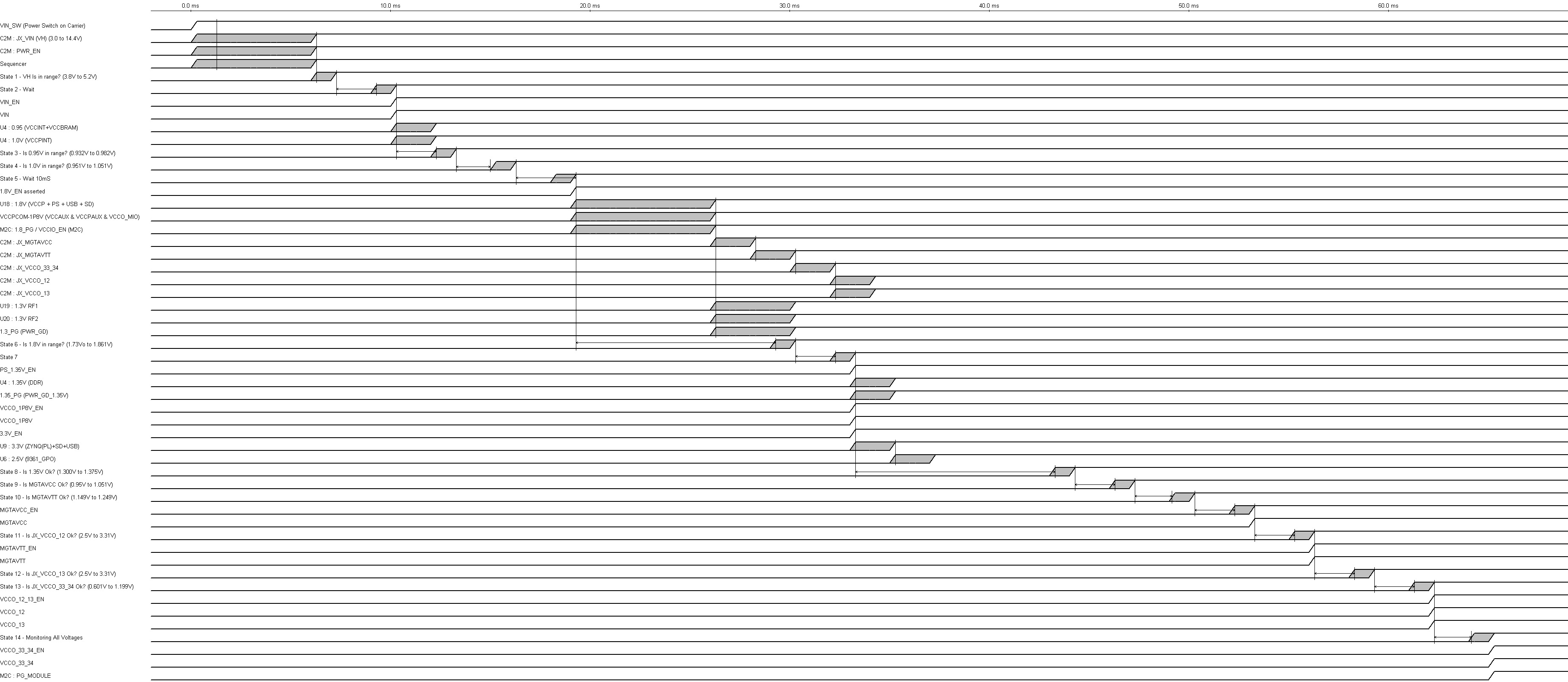 The tool used to generate this diagram isTiming Diagram Editor
State Diagram
The state diagram is available in pdf format sequencer_state_diagram.pdf.

Programming the ADM1166 Power Sequencer
Using Linux or Hyperterminal Program
Required items
- A 12V, 5A AC-DC Power Adapter.
- 1 PicoZed SDR Carrier Board (AES-PZSDRCC-FMC-G).
- 1 PicoZed SDR Board (AES-PZSDR-Z7035-AD9361-G).
- 1 microSD card or 1 SD card.
- 1 micro USB cable.
- 1 Ethernet cable.
Setting up the Hardware
- Plug the PicoZed SDR into the PicoZed SDR Carrier.
- Plug the power supply into connector P20.
- Plug the micro USB cable into connector P10.
- Plug the ethernet cable into your network and the PicoZed SDR Carrier.
- Insert the micro SD card into the PicoZed SDR.


Command Line
In the command line of your favorite terminal program, enter the following:
root@analog:~#git clone https://github.com/analogdevicesinc/PicoZed-sdr.git
Cloning into 'PicoZed-sdr'...
remote: Counting objects: 13, done.
remote: Compressing objects: 100% (11/11), done.
remote: Total 13 (delta 2), reused 0 (delta 0), pack-reused 0
Unpacking objects: 100% (13/13), done.
Checking connectivity... done.
root@analog:~# cd PicoZed-sdr/
root@analog:~# cd SDR2_ADM1166_updates/
root@analog:~# chmod +x ./adm1166_eeprom
root@analog:~# ./adm1166_eeprom ADM1166.hex
Starting to reprogramm the AD1166 EEPROM.
Reading f800 ... success
 ... existing memory is identical.
Reading f820 ... success
 ... existing memory is identical.
Reading f840 ... success
 ... existing memory is identical.
Reading f860 ... success
 ... existing memory is identical.
Reading f880 ... success
 ... existing memory is identical.
Skipping reserved page f8a0
Skipping reserved page f8c0
Skipping reserved page f8e0
Reading f900 ... success
 ... existing memory is identical.
Reading f920 ... success
 ... existing memory is identical.
Reading f940 ... success
 ... existing memory is identical.
Reading f960 ... success
 ... existing memory is identical.
Reading f980 ... success
 ... existing memory is identical.
Skipping reserved page f9a0
Skipping reserved page f9c0
Skipping reserved page f9e0
Reading fa00 ... success
 ... existing memory is identical.
Reading fa20 ... success
 ... existing memory is identical.
Reading fa40 ... success
 ... existing memory is identical.
Reading fa60 ... success
 ... existing memory is identical.
Reading fa80 ... success
 ... existing memory is identical.
Skipping reserved page faa0
Skipping reserved page fac0
Skipping reserved page fae0
Reading fb00 ... success
 ... existing memory is identical.
Reading fb20 ... success
 ... existing memory is identical.
Reading fb40 ... success
 ... existing memory is identical.
Reading fb60 ... success
 ... existing memory is identical.
Reading fb80 ... success
 ... existing memory is identical.
Skipping reserved page fba0
Skipping reserved page fbc0
Skipping reserved page fbe0
Successfully reprogrammed the ADM1166 EEPROM.
 ... reboot the board to load the new configuration.
root@analog:~#
Reboot the board and the new EEPROM configuration will be implemented.
Using the USB-SDP-CABLEZ serial I/O Interface
Required items
- A 5V, 2A AC-DC Power Adapter.
- 1 Breakout Board.
- 1 PZSDR Board.
- 1 microSD card (with appropriate image).

- 1 Custom Adapter for the USB-SDP-CABLEZ.

Software Setup
- Install the ADMxxxx Run Time Installer.
- Install the Super Sequencer Configuration Tool.
- Install the Graphviz setup.
- This is included in the install process of the Super Sequencer Tool and allows generation of state diagrams.
Hardware Setup
- Insert the micro SD card into the PZSDR board.
- Firmly plug the PZSDR board into the Breakout board.

- Using a USB mini cable, plug the USB-SDP-CABLEZ into the PC.
- Connect the custom adapter to the USB-SDP-CABLEZ.
- If using the carrier board, place a piece of non conductive tape on the bottom of the adapter board. It helps to avoid unintentional short circuits.

- If using the breakout board, or the PZSDR card by itself, no tape is required on the bottom of the adapter board.
- Plug the adapter into connector P1 on the PZSDR board, found on the underside of the PCB. Line up the 5 pins with the 5 holes of the connector.

- Check that the green LED seen in the image below is on meaning the boards are correctly mated.

- It is important to note, if the PZSDR board is not plugged into the break out board, the sequencer tool can not monitor the voltage rails. However, it can still be properly programmed. To monitor the voltage rails using the super sequencer tool, plug the PZSDR board into the break out board and toggle S5 so the switch is towards the outside edge of the board.


How to Program the Sequencer
- Find and open the Super Sequencer Software.
- The ADM1166 should be listed under device type.
- If the ADM1166 is not listed, check the connection between connector P1 of the PZSDR board and the custom adapater. A solid connection is required for configuration.

- Click 'Continue'.
- If prompted to load settings from last saved session, click 'No'

- Click 'File'.

- Click 'Recall Settings from File'.
- Click 'Recall'.
- Navigate to the desired .txt file and select it.
- Click 'Recall'.
- Click 'Ok'.
- Now wait a few seconds as the software works to import your configuration ADM1166.
- A prompt should appear detailing the checksum results.

- Click 'Ok'.
- Click 'EEPROM OPTIONS'.
- Click 'Copy Entire Configuration to EEPROM'.
- Now wait a few seconds as the software works to upload your configuration to the ADM1166.
- Once these steps are completed, the sequencer will be properly configured and the tool can be used to alter the configuration and observe the voltage rails.
- Disconnect the custom adapter from the PZSDR board.


Something went wrong... what can I do?
In the event you are staring at a PCB with no power, don't panic, there are options! The easiest thing to do is to plug in your USB-SDP-CABLEZ, as detailed in the instructions above. Navigate to the 'Readback' tab. From here you can observe each of the VH, VPx, VXx input voltages as read by the ADM1166.

Software Settings - Input Voltage Range Determination and Setting
The following provides a detailed overview on how the ADM1166 input voltage ranges are calculated and programmed to account for input and output ZYNQ voltage settings, ADM116 power sequencer input voltage ranges etc.
ZYNQ I/O Voltage Range
Starting with the XC7Z035 ZYNQ Zynq-7000 All Programmable SoC: DC and AC Switching Characteristics we see the following I/O voltage ranges for the banks of the ZYNQ.
| Description | VIN_MIN | VIN_MAX |
|---|---|---|
| VMGTAVCC | 0.97 V | 1.080 V |
| VMGTAVTT | 1.17 V | 1.230 V |
| VCCO (HR Bank) | 1.14 V | 3.465 V |
| VCCO (HP Bank) | 1.14 V | 1.890 V |
ADM1166 Super Sequencer Input Voltage Ranges
The ADM1166 has several input voltage ranges for the VP pins and VX pins. The VX pins only work on the Ultra-Low Range setting.
| ADM1166 Range | VP_MIN | VP_MAX | VX_MIN | VX_MAX |
|---|---|---|---|---|
| Mid-Range | 2.5000 V | 6.000 V | X | X |
| Low Range | 1.250 V | 3.000 V | X | X |
| Ultra-Low Range | 0.573 V | 1.375 V | 0.573 V | 1.375 V |
VMGTAVCC and VMGTAVTT drive directly into the VX3 and VX4 pins of the ADM1166. The I/O voltage range lines up nicely inside input voltage range of the sequencer. 1.14V is above the minimum voltage of the Ultra-Low Range (0.573V) and 1.23V is below the maximum voltage of the Ultra-Low Range (1.375V).
The Problem!
Unfortunately the VCCO I/O voltage levels don’t fit inside any one range of the sequencer. 1.14V is below the minimum voltage of the Low-Range (1.25V), and the 1.89V/3.465V is above the maximum voltage of the Ultra-Low Range (1.375V).
Fixing the problem for HP Banks 33 and 34
A resistor divider is added between the bank voltage and the ADM1166 input. The input impedance of the IC to ground (R3) is in parallel with R2.

Its resistance varies from 20k to 60k depending on the input voltage to the device. The information below is for a single part, not including temperature, supply or any other variation.

The resistor divider was designed so the worst case output voltage fits inside the Ultra-Low Range. Some iteration and simulation was done to determine the input impedance of the device for each particular voltage setting.
- When JX_VCCO_33_34 = 1.14V, the input impedance of the IC is 35k.
- When JX_VCCO_33_34 = 1.89V, the input impedance of the IC is 23k.
Calculating the parallel impedance of R2 and R3.
| Description | Ohms | Ohms |
|---|---|---|
| R2 | 10.0k | 10.0k |
| R3 | 35k | 23k |
| R2 P R3 | 7.777k | 6.96k |
Revisiting good old’ Ohm’s law gives:
- JX_VCCO_33_34_SEQ = (1.14V * 7777) / (4020+7777) = 0.7515V
- JX_VCCO_33_34_SEQ = (1.89V * 6969) / (4020+6969) = 1.198V
Both of these values are inside the Ultra-Low Range input voltage setting of the power sequencer.
Fixing the problem for HR Banks 12 and 13
Now to look at the resistor dividers for bank 12 (HR bank). Bank 13 is also an HR bank with the same resistor divider so the calculations are identical for it, and will not be replicated. The resistor divider was designed so the output voltage fits inside the Mid-Range, kind of. The resistor values are swapped and the bottom leg of the divider is connected to a 3.3V supply found on the PCB.

Now for some nodal analysis!
- I(R1) = (VOUT - V1)/(R1)
- I(R2) = (V2 - VOUT)/(R2)
- I(R3) = (VOUT)/(R3)
- I(R2) - I(R1) = I(R3)
- (V2-VOUT)/(R2) - (VOUT-V1)/(R1) = [(VOUT)/(R3)]
- Multiply everything by R1*R2*R3.
- (V2*R1*R3) - (VOUT*R1*R3) - (VOUT*R2*R3) + (V1*R2*R3) = (VOUT*R1*R2)
- Collect all Vout terms on the same side.
- (VOUT*R1*R2) + (VOUT*R2*R3) + (VOUT*R1*R3) = (V2*R1*R3) + (V1*R2*R3)
- VOUT*[(R1*R2) + (R2*R3) + (R1*R3)] = (V2*R1*R3) + (V1*R2*R3)
- VOUT = [(V2*R1*R3) + (V1*R2*R3)] / [(R1*R2) + (R2*R3) + (R1*R3)]
Now, just fill in the variables.
For the smallest possible ZYNQ output voltage and smallest possible ADM1166 input impedance.
- VOUT = [(V2*R1*R3) + (V1*R2*R3)] / [(R1*R2) + (R2*R3) + (R1*R3)]
- VOUT = 2.431V
The input impedance of the IC is found from the same graph as above.
This shows the smallest possible output voltage of the ZYNQ does NOT sit in the Mid-Range setting. So the minimum input for this range is 2.5V. This will accommodate most use cases.
If you are trying to use 1.2V for the HR bank 12 or bank 13, YOU MUST CHANGE to the low range setting.
Repeat….
If you are trying to use 1.2V for the HR bank 12 or bank 13, YOU MUST CHANGE to the low range setting.
For the largest possible ZYNQ output voltage and largest possible ADM1166 input impedance.
- VOUT = [(V2*R1*R3) + (V1*R2*R3)] / [(R1*R2) + (R2*R3) + (R1*R3)]
- VOUT = 3.041V
This shows the largest ZYNQ output voltage for the HR banks sits inside the Mid-Range, after going through the resistor divider.
So what does it all mean?
This table summarizes the final results including 1% resistor tolerance. The MGTAVCC and MGTAVTT already fit into the ultralow range of the sequencer. In order for the HR and HP banks to fit inside the ADM1166 input range, a resistor divider must be used to divide down the VCCO_12, VCCO_13 and VCCO_33_34 voltages.
| Zynq Voltage Rail | ADM1166 Range | Datasheet Min | Datasheet Max | Divider Vout Min | Divider Vout Max | ADM1166 Input Min | ADM1166 Input Max |
|---|---|---|---|---|---|---|---|
| VMGTAVCC | Ultralow | 0.970 V | 1.080 V | X | X | 0.573 V | 1.375 V |
| VMGTAVTT | Ultralow | 1.170 V | 1.230 V | X | X | 0.573 V | 1.375 V |
| VCCO (HR Bank) | Mid-Range | 1.140 V | 3.465 V | 2.671 V | 3.348 V | 2.500 V | 6.000 V |
| VCCO (HP Bank) | Ultralow | 1.140 V | 1.890 V | 0.808 V | 1.356 V | 0.573 V | 1.375 V |
Resistor divider values
The table below summarizes the resistor values used in the PicoZed SDR SOM 2 design. All resistors are 1%.
| Description | ADM1166 Range | V1 | R1 | R2 | V2 |
|---|---|---|---|---|---|
| VCCO (HR Bank) | Ultralow | 1.140 V | 10.0k | 4.02k | 3.300 V |
| VCCO (HR Bank) | Ultralow | 3.465 V | 10.0k | 4.02k | 3.300 V |
| VCCO (HP Bank) | Mid-Range | 1.140 V | 4.02k | 10.0k | 0.000 V |
| VCCO (HP Bank) | Ultralow | 1.890 V | 4.02k | 10.0k | 0.000 V |
So… how do I setup the sequencer?
No worries… when a user purchases the PicoZed SDR 2×2 SOM, the sequencer comes pre-programmed with all of this information! If so inclined, you can change these settings by opening the software and utilizing the USB-SDP-CABLEZ dongle available for purchase from the ADI website. The pictures below show the default states for the voltage rails discussed in this adventure!
JX_MGTAVCC

JX_MGTAVTT

JX_VCCO_12

JX_VCCO_13

JX_VCCO_33_34

The ADM1166 Super Sequencer Software shows where to select the range for each input pin (VP or VX), how to set the desired UV/OV thresholds, hysteresis on these thresholds, what fault type to look for and a glitch delay.
But wait… the calculated tables are slightly different from the software values!
The thresholds are programmed using 8-bit resolution so the program was written to be as close to the UV or OV threshold, without restricting the range at all.
This looks great, but, I need to change some settings for my custom carrier.
Thinking of modifying the VH Thresholds? Be very careful! They are designed based on the FMC Carrier to account for diode voltage drop over current and temperature. Thinking of modifying other settings? Still be careful! This is not to say DON’T change settings, merely… think twice, then think twice more, then program once.
I programmed twice and thought once.
Did you adjust a setting incorrectly? Now the sequencer won’t allow the system to boot up because you typed the under voltage threshold into the over voltage threshold field? This is not a problem. If you have the USB-SDP-CABLEZ dongle, go here, do some more reading and you will be back up and running in no time. If you DON’T have a USB-SDP-CABLEZ dongle… you modified the sequencer software through some other means … take a deep breath… relax… then order a USB-SDP-CABLEZ dongle, go here, do some more reading and you will be back up and running in no time. The link provided gives significant detail on how to program the sequencer using the dongle or through a linux script.
Is there a default file I can load?
The default file that comes pre-loaded when you order hardware can be found on Github.
Navigation - PicoZed_SDR
Up: PicoZed_SDR
resources/eval/user-guides/pzsdr/power-and-sequencing.1472246555.txt.gz · Last modified: 26 Aug 2016 23:22 by Neil Wilson