


This version (26 Jan 2022 19:15) was approved by Naveen Afzal.The Previously approved version (22 Dec 2021 18:05) is available.
Table of Contents
EVAL-LTC4306-PMDZ User Guide
GENERAL DESCRIPTION
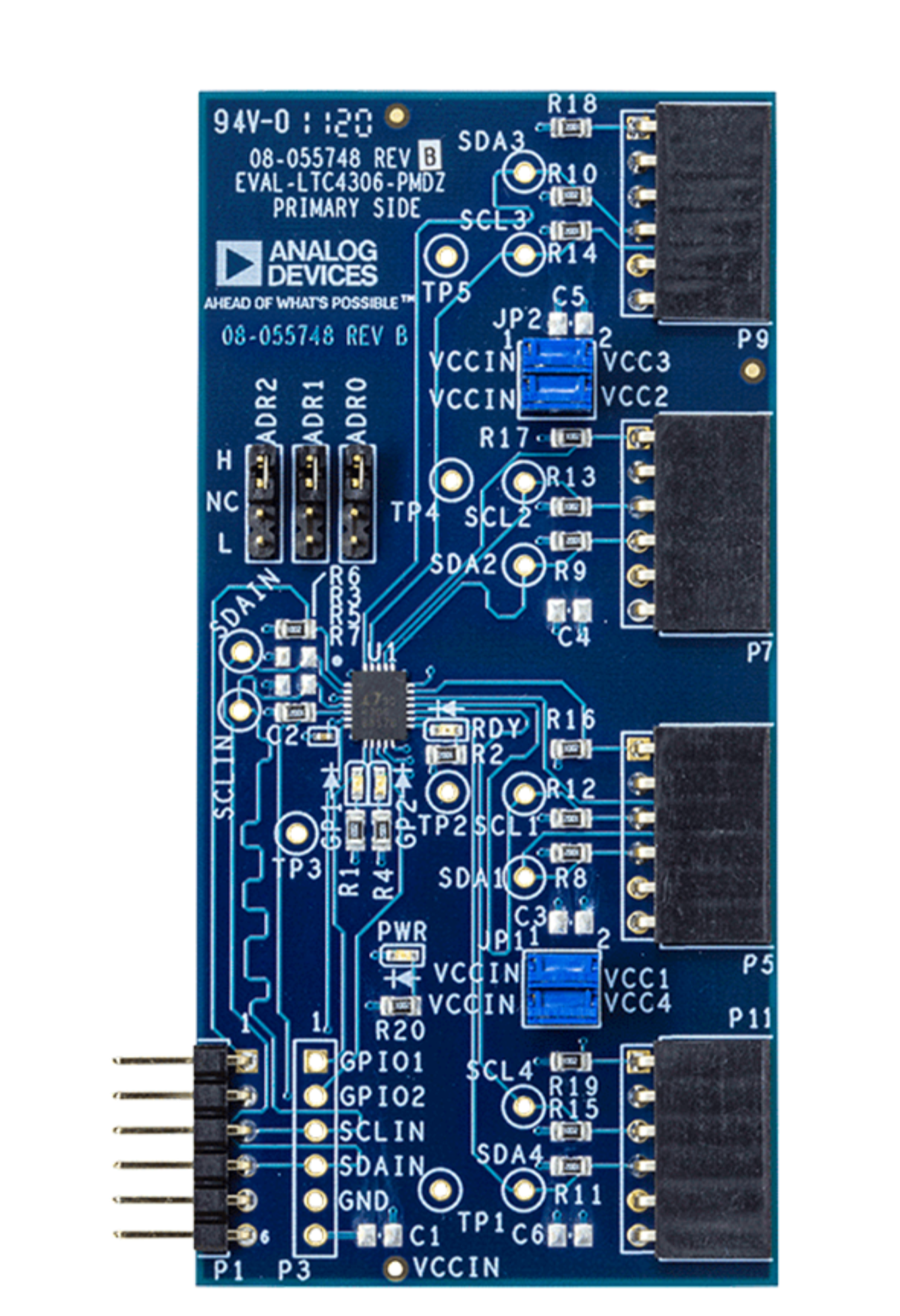
The EVAL-LTC4306-PMDZ features LTC4306, a 4-channel, 2-wire I2C bus and SMBus compatible multiplexer having bus buffers that provide capacitive isolation between the upstream bus and downstream buses.
This evaluation board provides 6-pin PMOD connectors for upstream and downstream connection for compatibility with PMOD form factors such as EVAL-ADICUP3029, an Arduino based Wireless Development Platform for Internet of Things applications based on an ultra-low power ARM Cortex-M3 processor.
Pmod™ is the Digilent defined standard of Peripheral Modules, small I/O interface boards that offer an ideal way to extend the capabilities of programmable logic and microcontroller boards. They allow sensitive signal conditioning circuits and high-power drive circuits to be placed where they are most effective - near sensors and actuators.
- Through software control, the EVAL-LTC4306-PMDZ connects the upstream 2-wire bus to any desired combination of downstream buses, i.e. (SCL1, SDA1 : SCL4, SDA4).
- Each bus can be pulled up to a supply voltage ranging from 2.7V to 5.5V, independent or dependent of the LTC4306 supply voltage by placing jumpers in different settings.
- The downstream buses are also provided with their own ALERT_N input pins for fault reporting.
- Programmable timeout circuitry disconnects the downstream buses if the bus is stuck low. When activated, rise time accelerators source currents into the 2-wire bus pins during rising edges to reduce rise time.
- Two general purpose input/output (GPIO) pins (accessible via the P3 connector (Not soldered)) can be configured as inputs, open-drain outputs or push-pull outputs.
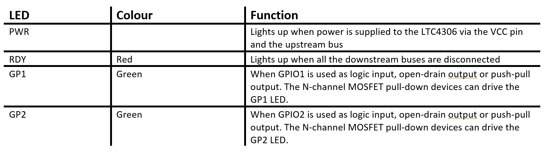
- LEDs on the board such as RDY, GP1 and GP2 allow fault monitoring and easy signal tracing.
- The reset or the ENABLE pin restores all device features to their default states when driven low and opens all the FET switches that connect the upstream to the downstream buses.
- Only three address pins (accessible via the ADR0, ADR1 and ADR3 pin headers) provide 27 distinct I2C addresses!
SPECIAL FEATURES
- 4 Selectable Downstream Buses: Nested addressing possible when used as a mux.
- Disconnect from Stuck Bus: Allows master to resume connection if one of the downstream bus is stuck low.
- 2-Wire Bus Buffers: Breaks up the upstream and downstream side into two buses; Also breaks up the capacitance.
- Buffer Supply Independence: Level-shifting is possible; 2-Wire buses can be pulled up to supply voltages ranging from 2.7V to 5.5V, independent of the LTC4306 VCC voltage
- Slew Limited Rise Time Accelerators help in reducing rise time: Allow the use of longer cables with less reflection and larger bus pull-up resistors for better noise margin.
- 2-Wire Bus Hot Swap: Prevents 2-wire bus corruption during live insertion and removal from backplane
- Fault Reporting: Helps master find and resolve system faults efficiently. For example, ALERT pins on upstream and downstream buses.
EVALUATION BOARD CIRCUITRY
EVAL-LTC4306-PMDZ comes with PMOD connectors on both upstream and downstream side for compatibility with PMOD form factors, 10K pull up resistors on upstream and all downstream buses and 0.1uF bypass capacitor on the upstream side. The user has the option to add 6 pin 2.54mm pitch pin header for connection to the GPIOs (General Purpose Input/Output pins) on EVAL-LTC4306-PMDZ for extra functionality. The user also has the option to add test points on different places on the board for fault monitoring and place additional bypass capacitors (0805 size footprint) on the upstream and the downstream side for defense against any unwanted noise in their system for adequate bypassing on power supply lines.
GENERAL OPERATION
For operation with EVAL-LTC4306-PMDZ, connect the master/host controller’s SDA and SCL pins to the LTC4306’s SDAIN and SCLIN pins (upstream bus pins) via the P1 PMOD connector. VCCIN (supply voltage of the LTC4306) can be anywhere from 2.7V to 5.5V (as shown in Figure 1). The host controller on the upstream side first addresses and configures the LTC4306 via I2c commands by writing to register 3 (see page 9 of the datasheet) to connect the upstream bus to one or more of the four downstream buses. Once the communication between the upstream and downstream buses are established, a master on the upstream 2-wire bus (SDAIN, SCLIN) can connect to any combination of downstream buses through the LTC4306’s bus buffers and multiplexers/switches. As a result, the same device address can be used on multiple downstream buses.
Each downstream bus can be powered up separately using its own VCC pin (VCC1:VCC4 on the schematic) on the P5:P11 connector. Hence, the LTC4306 can be used as a level shifter.
To power up all the downstream buses using LTC4306’s voltage supply, insert jumper JP1, JP2 in both A and B positions. Inserting jumper JP1 in A position connects the upstream voltage supply to the first downstream bus (SCL1, SDA1). Similarly, inserting jumper JP1 in B position connects the upstream voltage supply to the second downstream bus (SCL2, SDA2) and so on.
Additional configurations include enabling and disabling the rise time accelerators on the backplane side and/or the card side, setting the GPIOs to open drain output, push-pull output, or input mode, setting or resetting the GPIO’s outputs (to use GPIOs solder the P3 connector), disabling the Bus Stuck Low disconnect feature or setting the disconnect time to 7.5ms, 15ms, 30ms. A host controller can also read the internal registers of the LTC4306 to determine the settings of these features as well as fault statuses. All of these features are accessed by sending commands on the 2-wire bus.
The ENABLE pin, when pulled low, resets the LTC4306 to its registers default state and disables communication to it. Communication can be re-established when ENABLE is released high. By default, it is pulled up to VCCIN by a 10k resistor. However, the 2nd pin of the P1 PMOD connector can be used to set ENABLE pin low.
On the downstream side the slave devices should be able to report faults. The fault pins on each of the slave device on downstream buses 1-4 should connect their fault pins to ALERT1_N : ALERT4_N on the P5:P11 connectors, respectively. The LTC4306 passes downstream faults to the upstream host by pulling down on the ALERTX_N pin, so this host’s fault input should be connected to the LTC4306 ALERT_N pin.
When the upstream bus is connected to one or more downstream buses, the READY pin voltage is pulled up to VCC. When the upstream bus is disconnected from all downstream buses, the READY voltage is low and the red RDY LED should light up. On EVAL-LTC4306-PMDZ, the default setting for jumpers on ADR0, ADR1 and ADR2 is the right position. This connects all the ADR pins to VCCIN, which sets the address of the LTC4306 to 0xAA (in hexadecimal). To set a different address, configure the jumpers according to Table 1 of the data sheet on page 13 (note: left position = L, middle position = NC, right position = H; Disconnect = NC for all the 3 jumpers on each ADR0, ADR1 and ADR2).

Figure (1). EVAL-LTC4306-PMDZ set-up
IMPORTANT NOTES
Do not activate rise time accelerators on buses whose pull-up supply voltages are lower than VCC
Make sure logic low voltages forced on all clock and data pins are < 0.4V.
When activating multiple downstream buses that are powered from separate supply voltages, make sure that the LTC4306’s VCC voltage is less than or equal to the lowest downstream bus pull-up supply voltage
Make sure that the power supply voltages do not exceed 5.5V
CONNECTORS

JUMPERS

LEDS
TEST POINT LOCATIONS

GETTING STARTED
EVAL-LTC4306-PMDZ is easy to set up to evaluate the performance of the LTC4306. Refer to Figure 1 for proper measurement equipment setup and follow the procedure below:
- Power up the upstream side of the board and the LTC4306 via the P1.6 pin. Connect P1.5 to GND and P1.4 and P1.3 to SDA and SCL of the host controller respectively. If the host controller is available in a PMOD form factor, plug in the P1 PMOD connector into the six pin PMOD host connector of the controller.
- Power up the downstream buses 1-4 using separate power supplies or from the upstream side. To power all the buses using the upstream voltage supply, place both the jumper JP1 and JP2 in A and B positions. This will connect VCCIN to the VCC1-VCC4 of the downstream buses.
- Configure jumpers JP6 – JP8 to set the desired 2- wire bus address for the LTC4306 according to Table 1 on page 13 of the datasheet (note: left position = L, middle position = NC, right position = H; Disconnect = NC for all three jumpers). By default, the address 0xAA is selected.
- Connect the SCLx and SDAx of the desired downstream bus to the SCL and SDA pin of the peripheral/slave device.
- To close all the FET switches to enable communication to all the downstream buses, send in a SMBus write command to change each of the bit 4,5,6 and 7 on register 3 on the LTC4306 to 1.
- Now any slave on any of the downstream bus 1-4 can be addressed seamlessly with the data transparently transmitted from the controller to the peripheral/slave devices.
- To experiment with more features of LTC4306, use the SMBus Read Byte and Write Byte protocols in conjunction with the register definitions on pages 8 and 9 of the datasheet.
DEMO WITH ADICUP3029 AND A Digital SENSOR
List of Hardware:
- EVAL-LTC4306-PMDZ board
- EVAL-ADICUP3029 Evaluation board
- EVAL-ADT7420-PMDZ Digital Temperature sensor Evaluation board
- SDP-K1 controller board (Optional)
- Mirco USB to USB cable
- Windows® Vista 32-bit/64-bit, Windows 7 32-bit/64-bit, Windows 8 32-bit/64-bit, or Windows 10 32-bit/64-bit with USB 2.0 port
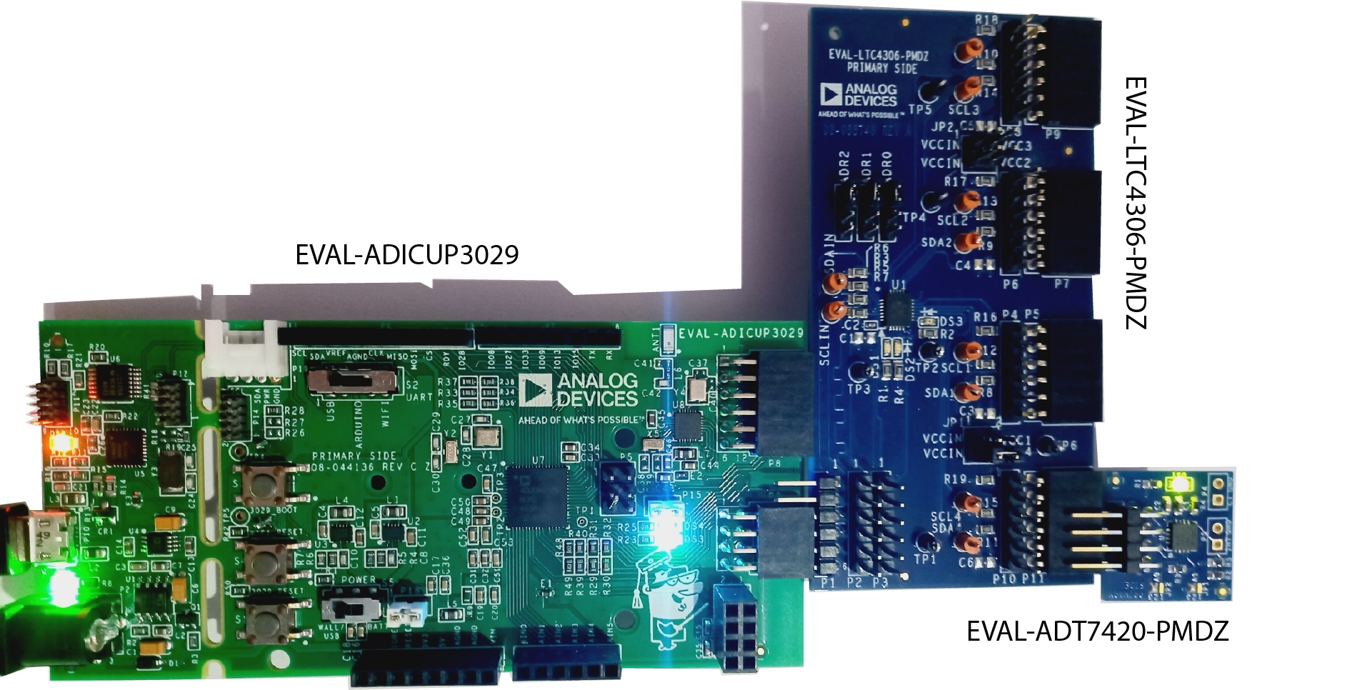
For this demo, the EVAL-ADT7420-PMDZ temperature sensor board was connected to the downstream bus number 4 on the EVAL-LTC4306-PMDZ.
Configuring the EVAL-LTC4306-PMDZ
Using the Bin A, binary file provided, program the SDP-K1 board whose SDA and SCL pins are connected to the upstream bus pins (i.e. SDAin and SCLin pins) on EVAL-LTC4306-PMDZ. This closes the FET switches on the desired downstream bus to allow communication between the upstream and the downstream devices. (If using your own sketch, do not forget to configure register 3 on the EVAL-LTC4306-PMDZ to close the FET switches on the desired downstream bus to allow communication between the upstream and the downstream devices. Make sure the LTC4306 device address is set to 0xAA (See page 13 of the datasheet for more information on how to set the address). This should switch off the red RDY LED on EVAL-LTC4306-PMDZ. If not, press the reset button on the SDP-K1 board and program it again.
Alternatively, EVAL-ADICUP3029 board can be used to close the FET switches of EVAL-LTC4306-PMDZ board. Plug the EVAL-LTC4306-PMDZ PMOD (P1) in the EVAL-ADICUP3029 base board, via the PMOD_I2C port (P9). Next, drag and drop the Hex A file provided into DAPLINK drive on your computer. This Hex A file programs the EVAL-ADICUP3029 board to configure and close the FET swtiches on EVAL-LTC4306-PMDZ. Like before, the red RDY LED should turn off on the EVAL-LTC4306-PMDZ indicating that one or more downstream channels is connected to the upstream bus as the FET switches are closed.
Configuring the EVAL-ADICUP3029 to receive data from EVAL-ADT7420-PMDZ
Next, plug the EVAL-LTC4306-PMDZ PMOD (P11) in the EVAL-ADT7420-PMDZ via the PMOD_I2C port (P1) on this digital temperature sensor. The yellow LED, DS1 should light up upon powering up this board.
The Figure below shows how the hardware should be set-up:
There are two basic ways to program the EVAL-ADICUP3029 with the software for the EVAL-ADT7420-PMDZ.
- Building, Compiling, and Debugging using CCES
Using the drag and drop method, the software is going to be a version that Analog Devices creates for testing and evaluation purposes. This is the EASIEST way to get started with the reference design.
Importing the project into CrossCore is going to allow you to change parameters and customize the software to fit your needs, but will be a bit more advanced and will require you to download the CrossCore toolchain.
The software for the ADuCM360_demo_adt7420 demo can be found here:
Software
Bin/Hex files
- Bin A, Binary file to program SDP-K1 to configure LTC4306
- Hex A, Hex file to program EVAL-ADICUP3029 to configure LTC4306 Not linked yet
- Bin B, Binary file to program EVAL-ADICUP3029 to read ADT7420
- Hex B, Hex file to program EVAL-ADICUP3029 to read ADT7420
Complete ADT7420 Source Files
For more information on importing, debugging, or other tools related questions, please see the tools user guide.
If going with option 2, the user needs to import adt7420_example_noos in their cross core studios workplace. To learn how to do that, visit this page cross core studios. Once imported, a debug configuration file needs to be set-up . (visit this page cross core studios for more information)
To see the temperature reading in the console, make sure ADI_APP_USE_BLUETOOTH is set to 0 in the header file (adt7420_app.h) before debugger is launched.
Once the debugger is launched, click on the resume button if the program is halted due to breakpoint shown below:
 The temperature sensor reading should now be displayed in the console. For detailed information on how to do this, visit the ADT7420 PMOD Temperature Demo page on analog wiki

DEMO WITH EVAL-SDP-CK1Z AND A COLOR SENSOR
For this demonstration, LTC4306 was used with EVAL-SDP-CK1Z (SDP-K1) Controller Board to read data out of an easily available color sensor from Adafruit industries, TC347525. The SDP-K1 controller board is a part of the evaluation system for many Analog Devices components and reference circuits. The SDP-K1 is a part of the system demonstration platform (SDP), which consists of a series of controller boards, interposer boards, and daughter boards. It is based on an STM32F469NI microcontroller. Mbed is used by Analog Devices to develop and distribute drivers for Analog ICs. Mbed is an online IDE developed by ARM. It is open-source and supports controller boards such as SDP-K1 with Cortex ARM core processors. On how to setup SDP-K1, please visit: mbed
List of Hardware:
- SDP-K1 controller board
- EVAL-LTC4306-PMDZ board
- I2C Color sensor/RGB sensor (For this example, TC347525 from Adafruit industries was used)
- 2 m, USB standard-A to mini-B cable
- Windows® Vista 32-bit/64-bit, Windows 7 32-bit/64-bit, Windows 8 32-bit/64-bit, or Windows 10 32-bit/64-bit with USB 2.0 port
- Jumper wires to connect different boards together
Set up the hardware as shown in the figure below. For this demo, the color sensor was connected to the downstream bus number 4 on the EVAL-LTC4306-PMDZ. (If using your own sketch, do not forget to configure register 3 on the EVAL-LTC4306-PMDZ to close the FET switches on the desired downstream bus to allow communication between the upstream and the downstream devices. The Hex device address was set to 0xAA (See page 13 of the datasheet for more information on how to set the address)

Software:
The program to configure the LTC4306 and the color sensor was compiled and a binary file was generated. This can be found in the resources section. To program the SDP-K1 board, connect the SDP-K1 board to your computer using the USB standard-A to mini-B cable. You should see the board as a new drive on your computer. Copy the binary file provided into the Mbed enabled board drive. You can also drag and drop the file, like a USB stick. After programming the SDP-K1 board, run the Colorsense.exe file. It can also be found in the resources section. A console and a GUI should pop up on the screen. Set the Baud rate to 9600 and enter your COM port number.
 Hit the return button on the console and the enter button on the GUI to make the user prompt frame disappear.
 You should now be able to see different colors appear on the screen as objects are held over the sensor.

Schematic, PCB Layout, Bill of Materials
Resources
Additional Information and Useful Links
resources/eval/user-guides/interface-isolation/eval-ltc4306-pmdz.txt · Last modified: 26 Jan 2022 19:15 by Naveen Afzal