


This version (13 Oct 2021 11:48) was approved by Naveen Afzal.The Previously approved version (11 Oct 2021 16:01) is available.
Table of Contents
EVAL-CN0564-ARDZ User Guide

INTRODUCTION
Monitoring and data acquisition systems require direct access to the sensors and actuators, preferably from a remote location and by means of a standardized communication method. With increased digitization and as industry 4.0 gain more ground, more analog sensors are being provided with a digital interface such as I2C or SPI. Digital signal integration is therefore increasing as they permit faster switch-on times and lower power consumption. In addition, further processing such as a wide variety of signal processing operations can be performed easily. I2C and SPI are examples of a highly ubiquitous and common digital interface that uses a synchronous serial communication. They are widely used for attaching lower-speed peripheral ICs to processors and microcontrollers in intra-board, short-distance communication.

The distance limitation is one of the key disadvantages of these interfaces. System designers have traditionally extended these interfaces using repeaters or drivers with a higher drive strength at the expense of increasing the overall cost and power consumption. These solutions may be inconvenient for many applications and have other disadvantages that negate their usability. For example, there could be large distances between point to point systems resulting in the ends of the connecting cables having differences in the local ground potentials. This can cause major issues and damage either the controller or the remote node.
The circuit shown in Figure (1) solves the problem of long distance, robust, SPI/I2C communication simply and easily without any sacrifices to circuit component count, operating speed, or software complexity. Ideal operation in high noise, harsh industrial environments require tolerance to large ground potential differences. The SPI/ I2C extenders feature robust transceivers which operate over an extended common mode range of ± 25V (for SPI communication) and ± 15V (for I2C communication) for distances up to 1200m. Each link consists of a single device at either end of the cable, capable of being powered from 3V to 5.5V, while a separate logic supply
allows the I2C or SPI interface to operate from 1.62V to 5.5V. The extenders also provide an internal control interface for fault monitoring, which is critically important when monitoring equipment over long distances.

Figure (1). EVAL-CN0564-ARDZ featuring LTC4331 and LTC4331 can be using with sensors such as the MEMS accelerometers for remote sensing as well as in conjunction with ADCs with SPI/I2C interface to read data from analog sensors for endless applications.
These extenders allow robust measurement and monitoring for many applications such as:
- Condition-based Monitoring
- Factory Automation
- Building Automation
- Structural Monitoring

and many more…
where remote sensing and increased distance between the measurement source and the control circuitry is a key design requirement for safety purposes when monitoring conditions in a harsh environment.
SYSTEM TOPOLOGY
The EVAL-CN0564-ARDZ uses LTC4331 and LTC4332 to extend I2C/SPI signals up to 1200m.
The LTC4331 enable data transmission required for I2C communication between two devices. It encodes I2C signals from the controller into differential signals with up to 1 MHz which are then transmitted through the twisted pair of cables. At the remote end of the cable, the differential signals are received again by another LTC4331 and decoded into I2C signals again, which are then routed to the peripheral.
Similarly, the LTC4332 enable data transmission required for SPI communication between two devices. It encodes SPI signals from the controller into differential signals with up to 2 MHz which are then transmitted through the twisted pair of cables. At the remote end of the cable, the differential signals are received again by another LTC4332 and decoded into SPI signals again, which are then routed to remote peripheral device.
Long Distance Communication
1. Fault protection
Both LTC4331 and LTC4332 have a ±60V fault protected differential transceiver that allows I2C/SPI communication over a single twisted pair differential link up to 1200m.
2. Extended Common mode range
The transceiver operates over an extended common mode range of ± 25V for LTC4332 (SPI extenders) and ± 15V for LTC4331 (I2C extenders) making it suitable for noisy environments or systems with ground potential differences.
3. ±40kV HBM on Interface pins + ESD/EFT protection
The link interface pins A, B, Y, Z on LTC4332 and A, B on LTC4331 feature protection to ±40kV HBM with respect to GND, VCC (with a 4.7μF capacitor to GND), A or B/ A, B, Y, or Z without latchup or damage, during all modes of operation or while unpowered.
Both LTC4331/LTC4332 also have an improved ESD protection that provides a high level of protection in the IEC ESD and EFT (Electrical Fast Transient) tests. Combined with the HBM test, the IEC tests help ensures that the LTC4331/LTC4332 are robust under a wide range of real world hazards and capable of transmitting signals from a long distance.
Selectable Baud rates
For a given SPEED setting, cable length specifications given in Table 2 of the LTC4331/LTC4332 datasheet must be adhered to or the they will not link
Selectable baud rates over the cable allow balancing performance with cable length specific to the application. In the case of I2C communications, the LTC4331 (local) – LTC4331 (remote) link is transparent; the remote slave devices appear as local devices to a local master. However, in the case of the SPI extender solution, the LTC4332 (local) – LTC4332 (remote) incurs a one-word latency during read accesses only. Physically distant devices would need a dramatically reduced clock rate to accommodate the prop. delay within each bit width. To overcome this limitation, the LTC4332 introduces a shift register into the MISO signal path.
The SPI read command needs to be extended by one byte. If not, the last byte will be lost in the LTC4332 MISO shift register when the Slave select is de-asserted.
Because the data sent from the SPI master to the slave experiences the same delay as the master-initiated interface clock (SCK), both will remain in sync across the entire data link. In the opposite direction, however, the slave sends data (MISO) to the master only when the first clock edge reaches the slave. This data will experience a second delay on its way back to the master, so the slave data will be out of sync by twice the cable’s propagation delay. Physically distant devices would need a dramatically reduced clock rate to accommodate the prop. delay within each bit width. To overcome this limitation, the LTC4332 introduces a shift register into the MISO signal path.
 As a result, SPI write requests to remote slave devices are software transparent, but SPI read requests to remote slaves incur a one-byte latency, meaning the read command needs to be extended by one byte. If not, the last byte will be lost in the LTC4332 MISO shift register when the Slave select is de-asserted. The WORD_LENGTH register (0x5h)(See the register map in the Datasheet for LTC4332) indicative of the depth of the shift register in MISO signal path on LTC4332, dictates when a SPI Master will begin receiving valid data on the MISO. For example, if the WORD_LENGTH is 8, the user would begin receiving valid MISO data 8 clock cycles after the Slave Select is asserted.
Interrupt/Alert signals
The LTC4331/ LTC4332 also support an interrupt signals that are mirrored from the remote network to the local network using the differential link for fault monitoring.
Internal Slave/Control Interface
Both LTC4331 and LTC4332 feature an internal I2C/SPI slave that can be talked to by setting up an I2C address for this slave using the A1 and A2 pins on LTC4331 for I2C communication or by pulling the SSC pin low onLTC4332 for SPI communication. Only SPI mode 0 and 1 can be used to talk to this slave.
This slave can be used to change configuration settings of the SPI or the I2C link such as the SPI mode (Any SPI mode(0,1,2,3) can be selected for the three separate slave select pins, SS1, SS2 & SS3 on the LTC4332 by writing to an internal register by initiating a write transfer to the internal slave that can access those registers. The word length which dictates the depth of the shift register in MISO signal path can also be adjusted by initiating a write command to the WORD_LENGTH register through this internal slave. It can also be used to access the internal fault registers for debugging and error reporting.
Galvanic Isolation
Various level of isolation may be required in some systems where the primary side is referenced to a different voltage (e.g. -48V distributed power systems) while the secondary side is referenced to ground etc. The local LTC4331/LTC4332 can be galvanically isolated from the remote LTC4331/LTC4332 on EVAL-CN0564-ARDZ using digital isolators like the ADUM141E/ADUM140E.
Digital isolation allows components to have ground potential differences provided by the LTC4331 and LTC4332, and still maintain a communication link. Isolation also provides protection against high voltages or currents caused by the line surges or ground loops that can occur in a system with multiple grounds.
Complete galvanic isolation can also be achieved using both power and signal isolation techniques. The isolated power supply uses a transformer driver IC to drive a discrete transformer, along with a simple rectifier and low-dropout regulator (LDO) to clean up the isolated rail. An integrated data and power solution eliminates the need for a separate, isolated dc-to dc converter in isolated designs.
Figure (2) shows how the SPI extenders on EVAL-CN0564-ARDZ can be isolated using ADUM141E/ADUM140E and ADUM5020 .

Figure (2). Isolating the Master MCU from the local LTC4332 featured on EVAL-CN0564-ARDZ using ADUM141E/ADUM140E and ADUM5020
HARDWARE SET-UP
Equipment Needed
- USB Type A to USB Type B cable
- Jumper wires
- 3 V to 5.5 V supply

General Description
EVAL-CN0564-ARDZ features a local-remote pair of both LTC4331 and LTC4332. It has Arduino headers for easy evaluation and integration of its SPI and I2C extenders with the widely available Arduino UNO and other Arduino compatible devices. The remote-local pair can be split at the V-groove on the PCB. The remote LTC4331 / LTC4332 is designed such that it can be mounted on a mechanically optimized block, EVAL-XLMOUNT1. This block has resonance optimized up to 20kHz and can be used with accelerometer (Z) breakout boards such as the EVAL-ADXL35X, a breakout board for 3-Axis MEMS Accelerometers (e.g. ADXL357). This MEMS sensor will be used in a vibration sensing example demonstrated in this user guide for evaluating the SPI extenders of this evaluation board.

Powering up the local and remote side LTC4331 :
The EVAL-CN0564-ARDZ has a local-remote pair of both LTC4332 (SPI extenders) and LTC4331 (I2C extenders) which requires power supply on both sides of the board. The local side LTC4331 is powered via the VCC pin which is connected to both the 5V and the 3.3V pins on the Arduino header. A jumper is placed on the path so the user can either select from either 5V or 3.3V to power up the local side LTC4331. Inserting the P10 jumper such that the pin 1 and 2 are connected on the P10 header will select the 5V supply from the Arduino header. Inserting this jumper such that pin 2 and 3 are connected will select the 3.3V supply. VCC is bypassed with 4.7μF ceramic capacitor to GND.
VL, the Logic Supply Voltage of the local side LTC4331 is connected to the IOREF pin of the Arduino header. The logic supply voltage can range from 1.62V < VL < 5.5V. It is bypassed with 1μF ceramic capacitor to GND.
The remote side LTC4331's VCC pin can be powered up using the local side's VCC supply by connecting pin 1 of the P5 header to the pin 1 of the P4 header. This is connected to the power supply of the local side. It can also be powered up by connecting an external supply to either pin 1 of the P5 header or to the remote side LTC4331's VL pin which is connected to pin 5 of the P8 header. This is placed on the area of the EVAL-CN0564-ARDZ 's PCB with the remote side LTC4331. The VL pin is connected to the VCC pin on the remote side LTC4331 via R3, a solder on resistor. Therefore, powering up either of them will power up both the VCC and the VL pin of the remote side LTC4331 only. To power them up separately, de-solder the R3 resistor. Like the local side LTC4331, the remote side LTC4331 has its VCC pin bypassed with 4.7μF ceramic capacitor to GND and VL pin bypassed with 1μF ceramic capacitor to GND.

Figure (3). When R3 resistor is soldered on, the remote side VCC and VL are connected. The remote side can be powered up by either (1) By connecting the remote side VCC (pin 1 of the P5 header) to the local side VCC (pin 1 of the P4 header), (2) By connecting the remote side VCC (pin 1 of the P5 header) to an external power supply or (3) By connecting an external power supply to the remote side VL pin on pin 5 of the P8 header.
Remote Reset:
The ON pin on the local side LTC4331 can be used to trigger an internal reset which is held and outputs are disabled if it's de-asserted. The ON pin is connected to IOREF by inserting the P12 jumper such that its pin 1 and 2 are connected. This enables all the outputs and disables reset. Insert the P12 jumper such that its pin 2 and 3 are connected to trigger the internal reset which disables the outputs. If the P12 jumper is not inserted, the ON pin is controlled externally by an MCU via the Arduino header.
LINK AND RDY:
The Link pin outputs the Link Status. It is an Open-Drain Output. LINK is driven low after the LTC4331’s I2C interface has joined the I2C bus in addition to establishing link communication with the remote side. It is pulled up to IOREF internally. The DS4 LED lights up when the link is established. To monitor its status, this pin is connected to the D5 pin on the Arduino header via the JP5 jumper. Insert this jumper in position B to monitor the LINK status using an MCU externally.
On the remote side, the LINK pin is pulled up to the remote side VL through a 10k ohm resistor. The DS5 LED lights up when the remote link is established.
The RDY pin is an I2C Ready Status Open-Drain Output. RDY is driven low after the device’s I2C interface has joined the bus. It is used to detect when the LTC4331’s control interface is available in the absence of a connected link. The DS3 LED lights up when this happens. RDY is pulled up to IOREF via a 10k resistor.
The ALERT pin:
It is a SMBALERT/Interrupt signal for the LTC4331. ALERT is an open-drain output. Values set on the remote side ALERT propagate to the local side ALERT pin. In addition, ALERT is the SMBALERT function for the local side’s I2C control interface when enabled (i.e. The ALERT pin switches to a level-sensitive active low interrupt signal when register field INTR_MODE = 1). It is pulled-up to IOREF on the local side and Remote side VL on the remote side LTC4331 through a 10k resistor. To monitor its status using an MCU externally via the D3 pin on the Arduino header, insert jumper JP3 in position C. Do not insert this jumper if not used.
The CNTRL pin:
Values set on the local side CTRL pin propagate to the remote side CTRL pin over the differential link. On the remote side, CTRL is not driven at startup until the differential link is established. CTRL can be monitored using the CTRL test point. CTRL on the remote side LTC4331 is connected to pin 1 on the P8 header. This pin can be monitored on the remote side to determine if the differential link has been established.
Setting the I2C address for the internal slave on the local side LTC4331:
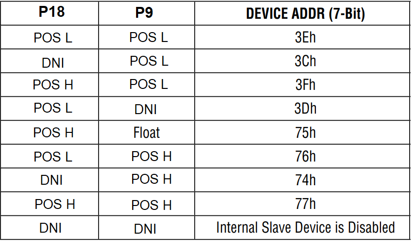
A1 and A2 are a 3-state input pins. A1 & A2 selects one of eight possible I2C addresses assigned to the internal slave device. Disconnect the P9 and the P18 jumper to disable the internal I2C slave device. Set to high, low, or float as defined in Table below. (POS H = Connect pin 1 and 2 of the header, POS L = Connect pin 2 and 3 of the P18/P9 header)
The SLO pin:
Local Side:
This is a slow Mode Input. To set it to low to limit the link transmitter slew rate which also limits the maximum
link rate set by SPEED1 and SPEED2, insert jumper P15 in POS L (connect pin 2 and 3 of the P15 header).
Insert jumper P15 in POS H (connect pin 1 and 2 of the P15 header) to disable it. Do not leave this jumper disconnected. SLO is referenced to GND and VCC and only valid for SPEED INDEX 0 and 1.
Remote side::
To set it to low to limit the link transmitter slew rate which also limits the maximum
link rate set by SPEED1 and SPEED2, solder the resistor JP11 in POS L (connect pin 2 and 3).
Solder the resistor JP11 in POS H (connect pin 1 and 2 of the P15 header) to disable it. Do not leave this resistor disconnected.
Speed 1 and 2:
Local Side:
Speed 1 and 2 correspond to the P16 and the P17 headers. To set speed 1 to High, insert the P17 jumper in POS H (connect pin 1 and 2 of the P17 header). To set it to Low, insert the P17 jumper in POS L (connect pin 2 and 3 of the P17 header). Disconnect this jumper to float the Speed 1 pin.
To set speed 2 to high, insert the P16 jumper in POS H (connect pin 1 and 2 of the P16 header). To set it to Low, insert the P16 jumper in POS L (connect pin 2 and 3 of the P16 header). Disconnect this jumper to float the Speed 2 pin. Refer to Table 2 on the LTC4331 datasheet to set Speed 1 and 2 to high, low or float to select a defined speed index.
Remote Side:
JP13 and JP12 are solder on resistors that can be soldered to select a speed index on the remote side. (Speed index on the remote side should match the speed index selected on the local side). To set speed 1 to high, solder the resistor JP14 in POS H (connect pin 1 and 2). To set it to Low, solder the JP14 resistor in POS L (connect pin 2 and 3). Do not solder on the JP14 resistor to float the Speed 1 pin on the remote side. Refer to Table 2 on the LTC4331 datasheet to set Speed 1 and 2 to high, low or float to select a defined speed index.
To set speed 2 to high, solder the resistor JP13 in POS H (connect pin 1 and 2). To set it to Low, solder the JP13 resistor in POS L (connect pin 2 and 3). Do not solder on the JP13 resistor to float the Speed 1 pin on the remote side. Refer to Table 2 on the LTC4331 datasheet to set Speed 1 and 2 to high, low or float to select a defined speed index.
Connect the local side LTC4331 to the remote side LTC4331:
Connect Pin 3 of the P4 header on the local side to Pin 3 of the P5 header on the remote side and Pin 4 of the P4 header on the local side to Pin 4 of the P5 header on the remote to connect the differential driver outputs on the local side to the differential receiver inputs on the remote side. R28 is a 110 ohm termination resistor that can be soldered or de-soldered. R27 is pulled up to VCC and R35 is pulled down to ground via 620 ohm resistors to implement fail-safe biasing.
SCL and SDA:
SCL and SDA are pulled up to IOREF through 2k ohm resistors on the local side.
On the remote side, SCL and SDA are pulled up to the remote side VL through 2k ohm resistors. Remote side LTC4331's SCL and SDA pins are connected to pin 3 and 4 of the P8 header. Connect the remote peripheral's SCL and SDA pins to these SCL and SDA pins on the P8 header.
Setting up the Evaluation board for SPI communication
Powering up the local and remote side LTC4332:
The EVAL-CN0564-ARDZ also features a local-remote pair of LTC4332 (SPI extenders) which requires power supply on both sides of the board. The local side LTC4332 is powered via the VCC pin which is connected to both the 5V and the 3.3V pins on the Arduino header. A jumper is placed on the path so the user can either select from either 5V or 3.3V to power up the local side LTC4331. Insert the P10 jumper such that the pin 1 and 2 are connected on the P10 header. This will select the 5V supply from the Arduino header. Inserting this jumper such that pin 2 and 3 are connected will select the 3.3V supply. VCC is bypassed with 4.7μF ceramic capacitor to GND.
VL, the Logic Supply Voltage of the local side LTC4332 is connected to the IOREF pin of the Arduino header. The logic supply voltage can range from 1.62V < VL < 5.5V. It is bypassed with 1μF ceramic capacitor to GND.
The remote side LTC4332's VCC pin can be powered up using the local side's VCC supply by connecting pin 5 of the P3 header to the pin 5 of the P6 header. This is connected to the power supply of the local side. It can also be powered up by connecting an external supply to either pin 5 of the P6 header or to the remote side LTC4332's VL pin which is connected to pin 7 of the P7 header. This is placed on the area of the EVAL-CN0564-ARDZ 's PCB with the remote side LTC4332. The VL pin is connected to the VCC pin on the remote side LTC4332 via R24, a solder on resistor. Therefore, powering up either of them will power up both the VCC and the VL pin of the remote side LTC4332 only. To power them up separately, de-solder the R24 resistor. Like the local side LTC4332, the remote side LTC4332 has its VCC pin bypassed with 4.7μF ceramic capacitor to GND and VL pin bypassed with 1μF ceramic capacitor to GND.

Figure (4). When R24 resistor is soldered on, the remote side VCC and VL are connected. The remote side can be powered up by either (1) By connecting the remote side VCC (pin 5 of the P6 header) to the local side VCC (pin 5 of the P3 header), (2) By connecting the remote side VCC (pin 5 of the P6 header) to an external power supply or (3) By connecting an external power supply to the remote side VL pin on pin 7 of the P7 header.
Remote Reset:
The ON pin on the local side LTC4332 can be used to trigger an internal reset which is held and outputs are disabled if it's de-asserted. The ON pin is connected to IOREF by inserting the P19 jumper such that its pin 1 and 2 are connected. This enables all the outputs and disables reset. Insert the P19 jumper such that its pin 2 and 3 are connected to trigger the internal reset which disables the outputs. If the P19 jumper is not inserted, the ON pin is controlled externally by an MCU via the Arduino header.
The LINK pin
The Link pin outputs the Link Status. It is an Open-Drain Output. LINK is driven low when the LTC4332 establishes link communication. It is pulled up to IOREF through a 10k ohm resistor. The DS2 LED lights up when the link is established. To monitor its status, this pin is connected to the D6 pin on the Arduino header via the JP5 jumper. Insert this jumper in position A to monitor the LINK status using an MCU externally.
On the remote side, the LINK pin is pulled up to the remote side VL through a 10k ohm resistor. The DS1 LED lights up when the remote link is established.
The INT pin:
INT is an open-drain output in local mode and an input in remote mode. Values set on the remote side INT propagate to the local side INT pin. In addition, INT is the level-sensitive active low interrupt signal for the LTC4332’s control interface. It is pulled-up to IOREF on the local side and Remote side VL on the remote side LTC4332 through a 10k resistor. To monitor its status using an MCU externally via the D2 pin on the Arduino header, insert jumper JP3 in position B. Do not insert this jumper if not used.
The SC pin:
This is the Control Interface Select Input (Active Low). SSC enables access to the LTC4332 internal control registers. When is use, insert the JP3 jumper in position D. SSC can be set low externally via the D4 pin on the Arduino header to initiate a SPI transfer to the internal slave device inside LTC4332 using pins SCK, MOSI, and MISO. SSC must be set high externally via the D4 pin on the Arduino header when the SPI bus is idle. SSC is only used on the local side LTC4332. SSC is weakly pulled to VL internally in LTC4332 and can be unconnected if not used. To leave it unconnected, disconnect the JP3 jumper in position D.
The SS_1 pin:
Remote Slave Select 1 (Active Low). When in local mode, SS1 is an input. Set SS1 low to initiate a remote SPI transfer to the remote peripheral device using pins SCK, MOSI, and MISO. SS1 can be set low externally via the D10 pin on the Arduino header. Connect the JP1 jumper in position D if D10 on the Arduino is configured as the Slave select pin. On the remote side LTC4332, SS1 is an output. Connect the remote SPI peripheral's chip select to pin 1 of the P7 header on the remote side LTC4332. SS1 must be set high when the SPI bus is idle. SS1 is weakly pulled to VL internally in LTC4332 and can be unconnected if not used.
Speed 1 and 2:
Local Side:
Speed 1 and 2 correspond to the P1 and the P2 headers on the local side. To set speed 1 to High, insert the P1 jumper in POS H (connect pin 1 and 2 of the P1 header). To set it to Low, insert the P1 jumper in POS L (connect pin 2 and 3 of the P1 header). Disconnect this jumper to float the Speed 1 pin.
To set speed 2 to high, insert the P2 jumper in POS H (connect pin 1 and 2 of the P2 header). To set it to Low, insert the P2 jumper in POS L (connect pin 2 and 3 of the P2 header). Disconnect this jumper to float the Speed 2 pin. Refer to Table 2 on the LTC4332 datasheet to set Speed 1 and 2 to high, low or float to select a defined speed index.
Remote Side:
JP4 and JP2 are solder on resistors that can be soldered to select a speed index on the remote side. (Speed index on the remote side should match the speed index selected on the local side). To set speed 1 to high, solder the resistor JP4 in POS H (connect pin 1 and 2). To set it to Low, solder the JP4 resistor in POS L (connect pin 2 and 3). Do not solder on the JP4 resistor to float the Speed 1 pin on the remote side. Refer to Table 2 on the LTC4332 datasheet to set Speed 1 and 2 to high, low or float to select a defined speed index.
To set speed 2 to high, solder the resistor JP2 in POS H (connect pin 1 and 2). To set it to Low, solder the JP2 resistor in POS L (connect pin 2 and 3). Do not solder on the JP2 resistor to float the Speed 1 pin on the remote side. Refer to Table 2 on the LTC4332 datasheet to set Speed 1 and 2 to high, low or float to select a defined speed index.
Connect the local side LTC4332 to the remote side LTC4332:
Connect Pin 1 of the P3 header on the local side to Pin 1 of the P6 header on the remote side, Pin 2 of the P3 header on the local side to Pin 2 of the P6 header on the remote side, Pin 3 of the P3 header on the local side to Pin 3 of the P6 header on the remote side and Pin 4 of the P3 header on the local side to Pin 4 of the P6 header on the remote side to connect the differential driver outputs and receiver inputs on the local side to the differential receiver inputs and driver outputs on the remote side. R7 and R8 are 110 ohm termination resistors for the local side receiver inputs and remote side receiver inputs respectively that can be soldered or de-soldered. R5 and R9 are pulled up to VCC and R6 and R10 are pulled down to ground via 620 ohm resistors to implement fail-safe biasing on the local and the remote side.
MISO, MOSI and SCK:
On the remote side, MISO, MOSI and SCK are connected to pin 3 and 4 and 5 of the P7 header. Connect the remote peripheral's MISO, MOSI and SCK pins to remote side MISO, MOSI and SCK pins on the P7 header.
Connectors and Jumper Configurations
I2C extender (LTC4331 local-remote pair)


SPI extender (LTC4332 local-remote pair)


Test Points

LEDS


ACCELEROMETER EXAMPLE USING THE SPI EXTENDER
The following section describes how the EVAL-CN0564-ARDZ was setup and tested for its SPI extender (Local LTC4332 -Remote LTC4332). The remote and the local side can be split at the V-groove as shown in the section above. Once split, the remote side of the board (i.e. featuring the remote LTC4332) can be mounted on a mechanically optimized block, EVAL-XLMOUNT1 (i.e. it has resonance optimized up to 20kHz). This can be used with accelerometer (Z) breakout boards such as the EVAL-ADXL357, a breakout board for 3-Axis MEMS Accelerometers featuring ADXL357.
In this example, EVAL-CN0564-ARDZ will be used with an Arduino UNO to read acceleration data with EVAL-ADXL357 for an easy evaluation of its SPI extenders.
Equipment Needed for this example

Getting Started
1. Download the Arduino sketch provided for evaluating either the SPI extenders on the EVAL-CN0564-ARDZ Evaluation Board and program the Arduino using it.
2. Plug in the EVAL-CN0564-ARDZ board into the Arduino Uno Rev 3

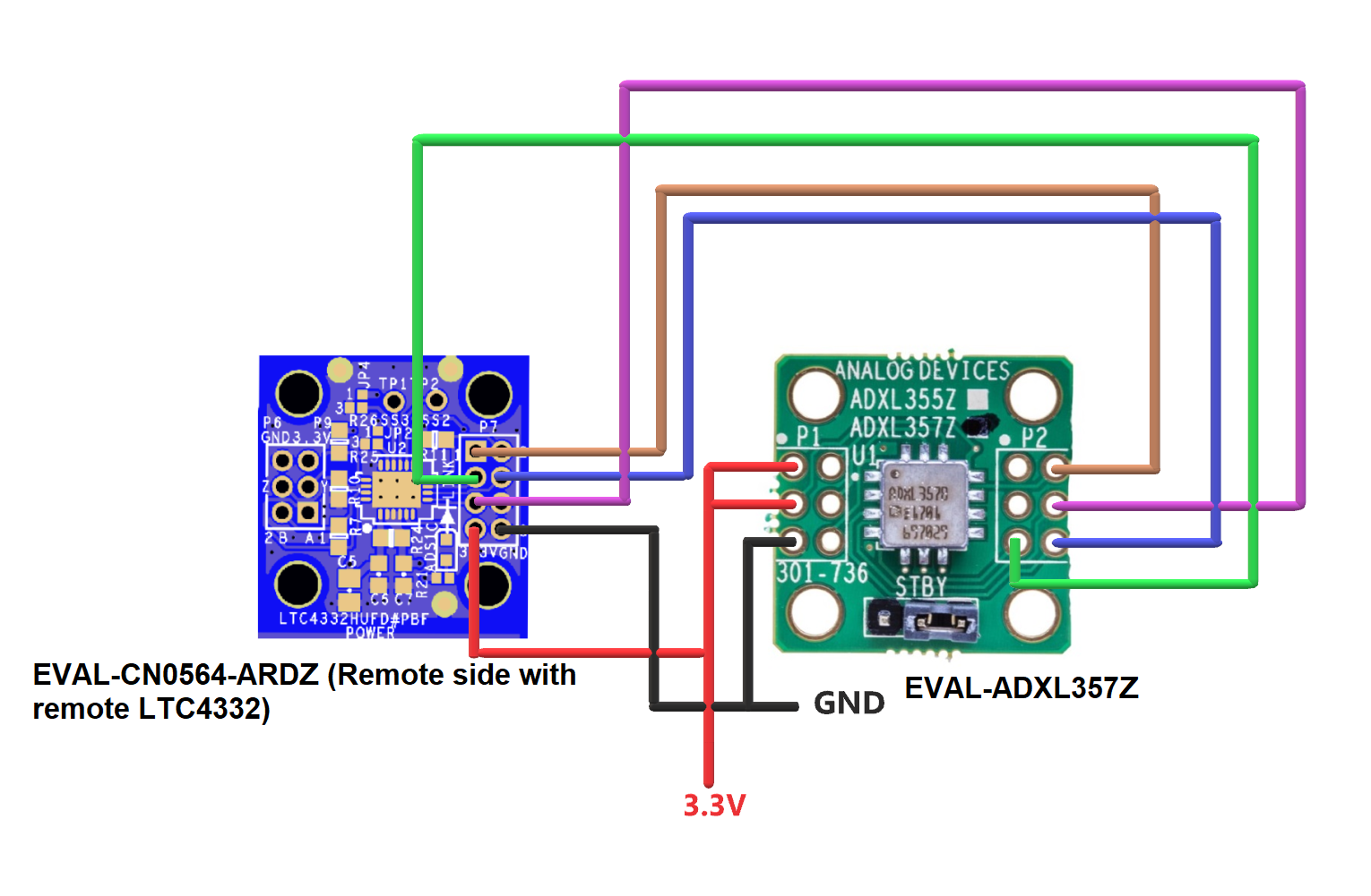
3. Connect the LTC4332 (Remote side) on the EVAL-CN0564-ARDZ to a MEMS ACCELEROMETER ON THE EVAL-ADXL357 as follows:
a. Solder the pin-header on to the EVAL-ADXL357 board. The 4-wire serial interface communicates in either the SPI or I2C protocol. The interface affectively autodetects the format being used, requiring no configuration control to select the format.
b. Connect the Remote slave select pin (Pin 1) of the P7 header on the EVAL-CN0564-ARDZ to the slave select pin (Pin 2) of the P2 header on the EVAL-ADXL357.
c. Connect the Remote MOSI pin (Pin 4) of the P7 header on the EVAL-CN0564-ARDZ to the MOSI pin (Pin 6) of the P2 header on the EVAL-ADXL357.
d. Connect the Remote MISO pin (Pin 3) of the P7 header on the EVAL-CN0564-ARDZ the MISO pin (Pin 5) of the P2 header on the EVAL-ADXL357.
e. Connect the Remote SCK pin (Pin 5) of the P7 header on the EVAL-CN0564-ARDZ to the SCK pin (Pin 4) of the P2 header on the EVAL-EVAL-ADXL357.
f. Connect the VDD pin (Pin 3) of the P1 header on the EVAL-ADXL357 to a 3.3V Power Supply.
g. Connect the VDDIO pin (Pin 1) of the P1 header on the EVAL-ADXL357 to a 3.3V Logic supply.
h. Connect the Remote VL (Pin 7) of the P7 header on the EVAL-CN0564-ARDZ to the 5V/3.3V Logic supply.
i. Connect pin 5 of the P1 header on the EVAL-ADXL357 to GND.
j. Connect the GND pin (Pin 8) of the P7 header on the EVAL-CN0564-ARDZ to GND. This is GND for the Remote LTC4332 side.
4. Make jumper Connections as follows:
a. P10 jumper should placed so the Pin 2 and 3 on P10 are connected on the EVAL-CN0564-ARDZ . This will select 5V power supply option.
b. JP1 jumper should be placed in position D to connect the Slave Select pin on the local LTC4332 to the D10 pin on the Arduino header.
c. JP5 jumper should be placed in position A to connect the Link pin on the local LTC4332 to the D6 on the Arduino header 2. Link is driven low when device establishes connection. It is pulled up to VIOREF internally to monitor status if VIOREF is supplied. If the Link pin is not used, float or connect to GND.
d. JP3 jumper should be placed in position B to connect the interrupt pin on the local LTC4332 to the D2 on the Arduino header. It is pulled up to VIOREF internally.
e. By default, Speed index 8 is selected on the remote LTC4332 (solder jumpers are used). The Speed index on the local side should be the same as the remote side.
f. P1 jumper should be placed in the position so its pin 2 and 3 are connected. Similarly, jumper P2 should also be placed in the position so its pin 2 and 3 are connected. This will select speed index 8 to match the speed index on the local side.
g. P19 jumper should be placed so its pin 1 and 2 are connected. This connects the ON pin on the local LTC4332 to IOREF. This will enable the input.

5. Connect LTC4332 (Local side) to the LTC4332 (Remote side) as follows:
a. Connect the Y pin of the P3 header (pin 1) on the Local LTC4332 side to the A pin of the P6 header (pin 1) on the remote LTC4332 side.
b. Connect the Z pin of the P3 header (pin 2) on the Local LTC4332 side to the B pin of the P6 header (pin 2) on the remote LTC4332 side.
c. Connect the A pin of the P3 header (pin 3) on the Local LTC4332 side to the Y pin of the P6 header (pin 3) on the remote LTC4332 side.
d. Connect the B pin of the P3 header (pin 4) on the Local LTC4332 side to the Z pin of the P6 header (pin 4) on the remote LTC4332 side.
e. Connect pin 6 of the P3 header to GND. This is GND for the Local side.
f. Pin 5 of the P6 header is remote side LTC4332's VCC power supply pin. As R24 is soldered on, remote side LTC4332's VL pin supplies power to this pin.
g. Connect pin 6 of the P6 header to GND. This is GND for the Remote side.

TEST
Mount the EVAL-ADXL357Z and the remote LTC4332 on the EVAL- XLMOUNT1 and turn on the power supplies that power up the boards. You should now be able to see 3 LEDS flash on the EVAL-CN0564-ARDZ board (2 LEDS on the local, 1 on the remote side). The X, Y and Z data read by the ADXL357 MEMS accelerometer (on the EVAL-ADXL357Z from the remote side) will be printed on the Serial Monitor. Download the Python .exe file and save it in a local directory. Exit the Serial Monitor and run the Python .exe file to see a real-time plot of the acceleration data.
The X, Y and Z acceleration (g) data is stored in three separate files by the python script and can be found in the same location containing the .exe file.

Real time acceleration data from ADXL357 can be plotted using the python .exe file:
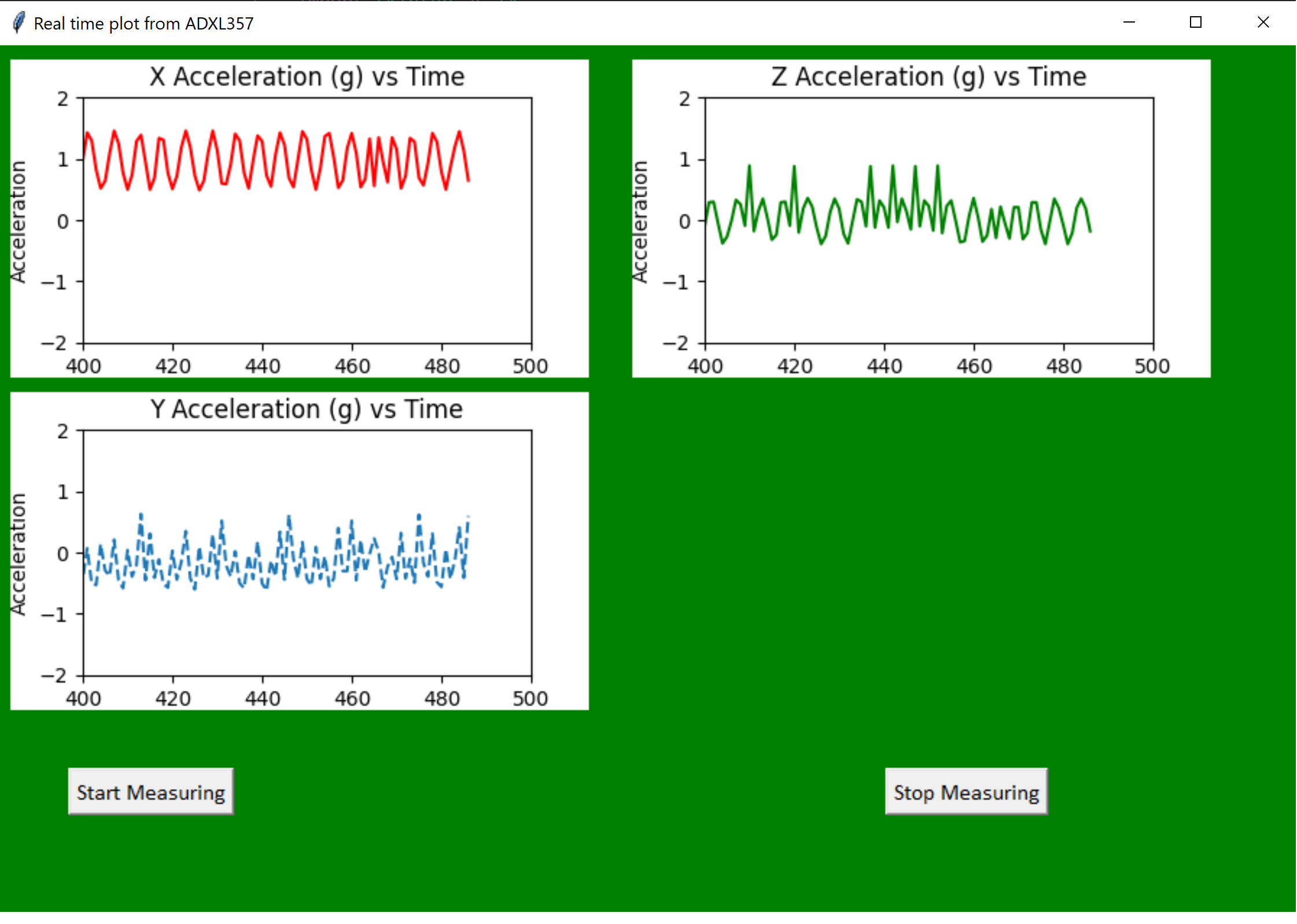
The user needs to enter their COM PORT and BAUD RATE when prompted by the console
Schematic, PCB Layout, Bill of Materials
Software
Additional Information and Useful Links
Reference Demos & Software
End of Document
resources/eval/user-guides/circuits-from-the-lab/cn0564.txt · Last modified: 13 Oct 2021 11:45 by Naveen Afzal