


This version (15 Nov 2023 03:41) was approved by Joyce Velasco.The Previously approved version (30 Jul 2021 07:19) is available.
Table of Contents
CN0198 — 5V Regulator Supplies High Transient Current for Dynamic Power Controlled DAC (DEPRECATED)
This particular reference design has been RETIRED or DEPRECATED, which means it is no longer supported. This page is here for historical/reference purposes only.
Overview
This circuit provides a unique power saving solution for a DAC-based 4 mA-to-20 mA output circuit. In order to provide sufficient headroom for typical resistive loads between 10 Ω and 1000 Ω, traditional 4 mA-to-20 mA output driver stages must operate on at least 20 V (plus some additional headroom) to provide a sufficient voltage to drive high value resistive loads. For low value resistive loads, however, the fixed value high voltage supply results in significant internal power dissipation that can affect DAC accuracy and require additional heat sinking.
General Setup
- AD5755 Evaluation board.
- ADP2300 Evaluation board.
- EVAL-SDP-CB1Z Evaluation board
- Power Supply: +/-15V supply.
- Digital Multimeter (Agilent 34401A)
- 1 GPIB-USB-HS
- 1 USB Type-A plug to USB Mini-B plug cable
Minimum PC/System Requirements
- One PC with the following
- Windows XP SP2, Windows Vista or Windows 7 Business/Enterprise/Ultimate editions
- Intel Pentium processor (x86 compatible), 1GHz or faster
- 512 MB RAM and 2 GB available hard disk space
- .NET 3.5 Framework
How to Install the Evaluation Software
- Extract the files within the file CN0198 SDP Eval Software.zip and open the file setup.exe. It is recommended that you install the CN0198 SDP Evaluation Software to the default directory path C:\Program Files\Analog Devices\CN0198\ and all National Instruments products to C:\Program Files\National Instruments\

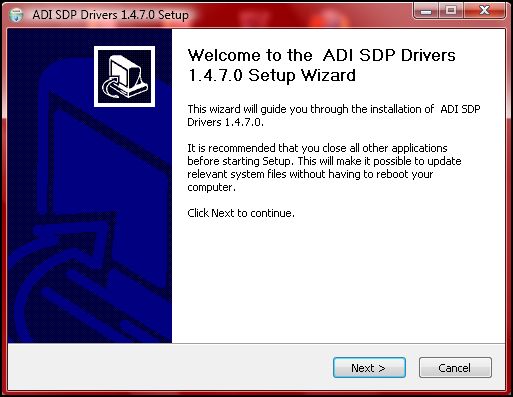
- Press “Next”.

- Press “Next”.

- Press “Next”.
- Upon completion of the installation of the CN0198 SDP Eval Software, the installer for the ADI SDP Drivers will execute. Follow the on-screen prompts to install the drivers. It is recommended that you close all other applications before clicking “Next”. This will make it possible to update relevant system files without having to reboot your computer.
- Press “Next”.
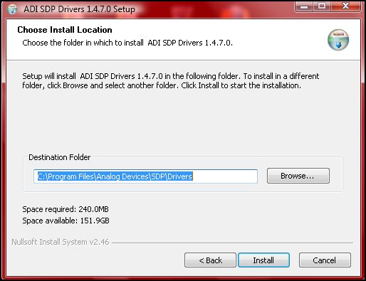
- It is recommended that you install the drivers to the default directory path C:\Program Files\Analog Devices\SDP\Drivers\
- Press “Next” to install the Drivers and complete the installation of all software necessary to evaluate the EVAL-CN0198-SDPZ


Step by Step Instruction for Connecting the Hardware
- Solder one end of a red wire to J1 of the ADP2300 and connect the other end to the +15V terminal of the DC power supply.
- Solder one end of a red wire to J2 of the ADP2300 and connect the other end to J6 - pin 2(PGND) of the AD5755 Evaluation Board.
- Solder one end of a black wire to J2 of the ADP2300 and connect the other end to the GND terminal of the DC power supply.
- Solder one end of a red wire to J3 of the ADP2300 and connect the other end to J6 - pin 1(AVCC) of the AD5755 Evaluation Board.

- Using a blue wire, connect J5 pin 1 of the AD5755 Evaluation Board to -15V connection of a DC power supply.
- Using a black wire, connect J5 pin 2 of the AD5755 Evaluation Board to the GND connection of a DC power supply.
- Using a red wire, connect J5 pin 3 of the AD5755 Evaluation Board to +15V connection of a DC power supply.
- Connect the EVAL-SDP-CB1Z Evaluation board to connector J9 of the AD5755 Evaluation Board.
- Plug the mini end of the USB cable into connector J1 of the EVAL-SDP-CB1Z Evaluation board.


AD5755 Evaluation Board Jumper Configuration
The following is a detailed description of how to configure jumpers LK0 - LK15 found on the AD5755 Evaluation Board.
Reference Selection: - Jumpers LK0, LK1, LK2 and LK3 determine the external reference voltage input for the AD5755-1. Only populate one jumper at any given time:
- LK0 selects the internal AD5755-1 reference.
- LK1 allows the user to input an off board reference voltage using terminal block J7 as an input.
- The reference input must fall between 4.95V and 5.05V to achieve performance specified in the datasheet.
- LK2 utilizes an on board +5V reference, the ADR02.
- LK3 provides power to the ADR02. If using LK0 or LK1, disconnect LK3.

Boost Voltage Selection - LK12, LK13, LK14, LK15 allow the connection of an external VBOOST supply.
- Populating LK12 and removing R43 connects the VBOOST pin of channel A to an external supply.
- If R43 is populated, the VBOOST pin for channel A is connected to the +15V supply.
- Populating LK13 and removing R44 connects the VBOOST pin of channel B to an external supply.
- If R44 is populated, the VBOOST pin for channel B is connected to the +15V supply.
- Populating LK14 and removing R17 connects the VBOOST pin of channel C to an external supply.
- If R17 is populated, the VBOOST pin for channel C is connected to the +15V supply.
- Populating LK15 and removing R20 connects the VBOOST pin of channel D to an external supply.
- If R20 is populated, the VBOOST pin for channel D is connected to the +15V supply.

+VSense Connections - LK4, LK6, LK8, LK10 connect the +Vsense input to Vout for Channel A, Channel B, Channel C and Channel D respectively.
- When LK4 is populated, the +Vsense input is connected directly to VOUTA.
- When LK4 is unpopulated, the channel A +VSense input is left floating and should be connected to the high side of the load resistance external to the board.
- When LK6 is populated, the +Vsense input is connected directly to VOUTB.
- When LK6 is unpopulated, the channel B +VSense input is left floating and should be connected to the high side of the load resistance external to the board.
- When LK8 is populated, the +Vsense input is connected directly to VOUTC.
- When LK8 is unpopulated, the channel C+VSense input is left floating and should be connected to the high side of the load resistance external to the board.
- When LK10 is populated, the +Vsense input is connected directly to VOUTD.
- When LK10 is unpopulated, the channel D +VSense input is left floating and should be connected to the high side of the load resistance external to the board.
-VSense Connections - LK5, LK7, LK9, LK11 connect the -Vsense input to ground for Channel A, Channel B, Channel C and Channel D respectively.
- When LK5 is populated, the channel A -Vsense input is connected directly to ground.
- When LK5 is unpopulated, the channel A -VSense input is left floating.
- When LK7 is populated, the channel B -Vsense input is connected directly to ground.
- When LK7 is unpopulated, the channel B -VSense input is left floating.
- When LK9 is populated, the channel C -Vsense input is connected directly to ground.
- When LK9 is unpopulated, the channel C -VSense input is left floating.
- When LK11 is populated, the channel D -Vsense input is connected directly to ground.
- When LK11 is unpopulated, the channel D -VSense input is left floating.

Opening and Enabling the Evaluation Software
- Launch the executable found at C:\Program Files\Analog Devices\CN0198. The software will automatically connect and display a prompt to the user.

- Press OK to close the prompt and arrive at the front panel of the evaluation software.
Programming Sequence and How to Enable the Output
- The sequence for correctly enabling the output is given in the flowchart below.

- The individual steps for enabling the output as described in the flowchart can be found below:
- In the DC-DC Control Register section click the Write button.
- In the DAC Control Register section, change the output type to 0-5V Voltage Range.
- In the DAC Control Register section click the Write button.
- In the Write to Data Register section, change the default word to FFFF.
- In the Write to Data Register section, click Write.
- In the DAC Control Register section, change the EN Output to Enabled.
- In the DAC Control Register section, click Write.
- Now, using a multimeter, you can probe the output channel of the device and will see approximately 5.00V.
Programming Sequence and How to Change the Output After Setting it to a Value
- The sequence for correctly enabling the output is given in the flowchart below.

- The individual steps for changing the output as described in the flowchart can be found below:
- In the DAC Control Register section, change the EN Output to Disabled.
- In the DAC Control Register section, click Write.
- In the Write to Data Register section, change the default word to 8000.
- In the Write to Data Register section, click Write.
- In the DAC Control Register section, change the EN Output to Enabled.
- In the DAC Control Register section, click Write.
Registration
Receive software update notifications, documentation updates, view the latest videos, and more when you register your hardware. Register to receive all these great benefits and more!
End of document
resources/eval/user-guides/circuits-from-the-lab/cn0198.txt · Last modified: 15 Nov 2023 03:40 by Joyce Velasco