


This version (08 Apr 2024 10:39) was approved by Samruth Krishna Kumar.The Previously approved version (11 Apr 2022 11:41) is available.
Table of Contents
Hardware Guide
Set-up Procedures
After following the instructions in the Software Procedures section, set up the evaluation and SDP boards as detailed in this section.
- Warning: The evaluation software and drivers must be installed before connecting the EV-AD4170-ASD1Z-U1 evaluation board and EVAL-SDP-CB1Z board to the USB port of the PC to ensure the PC correctly recognizes the evaluation system.
- Connect the EV-AD4170-ASD1Z-U1 to the controller board
- Option A: Connect the EV-AD4170-ASD1Z-U1 to the EVAL-SDP-CK1Z
- Using the 120 pin connector
- Screw the two boards together using the plastic screw-washer set included in the evaluation board kit to ensure that the boards are connected firmly together.
- Using the Arduino Connectors
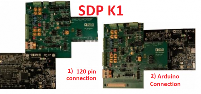
- Option B: Connect the EV-AD4170-ASD1Z-U1 to the EVAL-SDP-CB1Z
- Using the 120 pin connector
- Screw the two boards together using the plastic screw-washer set included in the evaluation board kit to ensure that the boards are connected firmly together.


Block Diagram

Hardware Link Options
| Link Numbers | Colour | Default Position | Descirption | Rough Board Location |
|---|---|---|---|---|
| LK1 | Blue | Inserted | Noise Test. Channels AIN5 + AIN6 | Right of J1 |
| LK2 | Red | Inserted | Thermocouple - Cold Junction Resistor Bypass | Right of J1 |
| LK3 | Red | Inserted | Precision Reference Resistor Bypass | Right of J1 |
| LK4 | Red | A | Pos A: GPIO 1 (IOUT1) to J1 Pos B: REFOUT | Right of J1 |
| LK5 | Blue | B | Wire Bridge EXC+ select: Pos A: MOSFET+ Pos B: AVDD | Right of J2 (EXC+) |
| LK6 | Blue | Uninserted | Short EXC+/REFIN+: Pos Inserted = 4 Wire Bridge | Right of J2 (4/6 wire) |
| LK7 | Blue | B | Wire Bridge EXC- select: Pos A: MOSFET- Pos B: Power Switch (GPIO1) | Right of J2 (EXC-) |
| LK8 | Blue | Uninserted | Short EXC-/AVSS: Pos Inserted = 4 Wire Bridge | Right of J2 (EXC-) |
| LK9 | Blue | Uninserted | Short EXC-/REFIN-: Pos Inserted = 4 Wire Bridge | Right of J2 (4/6 wire) |
| LK10 | Black | A | AD4595 AIN3+ AIN4. AVDD select. Pos A: Internal AVDD Pos B: External AVDD | Below of J5 (AMP34) |
| LK11 | Black | A | AD4595 AIN3+ AIN4. AVSS select. Pos A: Internal AVSS Pos B: External AVSS | Below of J5 (AMP34) |
| LK12 | Black | A | AD4595 AIN7+ AIN8. AVDD select. Pos A: Internal AVDD Pos B: External AVDD | Below of J5 (AMP78) |
| LK13 | Black | A | AD4595 AIN7+ AIN8. AVSS select. Pos A: Internal AVSS Pos B: External AVSS | Below of J5 (AMP78) |
| LK14 | N/A | DNI | SCP connect AC amplifier external AVSS and Ground | Left of J5 |
| LK15 | N/A | DNI | SCP connect external AVSS and Ground | Right of J5 |
| LK16 | N/A | DNI | SCP connect external AVDD and Ground | Right of J5 |
| LK17 | N/A | DNI | SCP connect external IOVDD and Ground | Right of J5 |
| LK18 | N/A | DNI | SCP connect AC amplifier external AVDD and Ground | Left of J5 |
| LK19 | Black | Uninserted | XTAL2 to Digital connector | Above PMOD (P6) |
| LK21 | Black | Inserted | Inserted: External crystal Uninserted External clock | Above SMB1 (Right) |
| LK22 | Blue | A | GPIO 0: Pos A: To Connector J4 Pos B: Mosfet | Below J4 |
| LK23 | Blue | A | GPIO 1: Pos A: To Connector J4/J2 (LK31) Pos B: Mosfet | Below J4 |
| LK24 | Red | A | GPIO 2: Pos A: To Connector J1 Pos B: Mosfet | Right of J2 |
| LK25 | Red | A | GPIO 3: Pos A: To Connector J1 Pos B: Mosfet | Right of J2 |
| LK26 | Black | A | ADXL1002 Test Pos A: Test Pos B:Standard | Below IOVDD LED (midle right) |
| LK31 | Blue | A | GPIO1 Connector select. Pos A: J2 (Power Switch) Pos B: J3 | Below J4 |
| LK32 | Black | A | IOVDD select. Pos A: 3.3V Pos B: EXT | Below J5 (near IOVDD LED) |
| LK33 | Black | A | LT1962-5 power down Pos A: On | Below J5 |
| LK34 | Black | A | LTC3129 power down Pos A: On | Below J5 |
| LK35 | Black | A | LT1962-2.5 power down Pos A: On | Below J5 |
| LK36 | Black | A | LTC1983 power down Pos A: On | Below J5 |
| LK37 | Black | A | ADP7182 power down Pos A: On | Below J5 |
| LK38 | Black | A | ADP150 power down Pos A: On | Below J5 |
| LK39 | Grey | Inserted | AVSS GND short | Top Left |
| LK40 | Grey | Inserted | AVSS GND short | Above Thermocouple Connection |
| LK41 | Grey | Inserted | AVSS GND short | Below J4 |
| LK42 | Grey | Inserted | AVSS GND short | Below J5 |
| LK43 | Grey | Inserted | AVSS GND short | Right of J1 |
| LK44 | Grey | Inserted | AVSS GND short | Below J5 (near AVDD LED) |
| LK45 | Grey | Inserted | AVSS GND short | Left of PMOD (P6) |
| LK46 | Grey | Inserted | AVSS GND short | Right of Thermocouple Connection |
| LKVOCM34 | Black | 4525 | VOCM ADA4945 Pos A: DACOUT Pos B: VBIAS Pos C: AD4525 Pos D: REFOUT | Right of Thermocouple Connection |
| LKVOCM78 | Black | 4525 | VOCM ADA4945 Pos A: DACOUT Pos B: VBIAS Pos C: AD4525 Pos D: REFOUT | Middle of board |
 Resistor Jumpers need to be modified for the selection of AC or DC inputs on AIN3-AIN4 and AIN7-AIN8, below is the guide on the resistor population for the selection of input type,
| AC/DC input | CH3-CH4 | CH7-CH8 |
| AC input | R41, R110 | R27, R40 |
| DC input | R42, R111 | R26,R39 |
 *For configuring AIN3-AIN4 as AC inputs resistors R41, R110 must be populated and R42, R111 must not be populated. Similarly for configuring AIN3-AIN4 as AC inputs resistors R42, R111 must be populated and R41, R110 must not be populated.
*For configuring AIN7-AIN8 as AC inputs resistors R27, R40 must be populated and R26, R39 must not be populated. Similarly for configuring AIN7-AIN8 as AC inputs resistors R26, R39 must be populated and R27, R40 must not be populated.
*For configuring AIN3-AIN4 as AC inputs resistors R41, R110 must be populated and R42, R111 must not be populated. Similarly for configuring AIN3-AIN4 as AC inputs resistors R42, R111 must be populated and R41, R110 must not be populated.
*For configuring AIN7-AIN8 as AC inputs resistors R27, R40 must be populated and R26, R39 must not be populated. Similarly for configuring AIN7-AIN8 as AC inputs resistors R26, R39 must be populated and R27, R40 must not be populated.
On Board Connections
Thermocouple Connector A1
Connector J1: DC (Analog Input)
Functionality:
- RTD
- Thermocouple
| Connection | Function |
|---|---|
| 1 | 1) IOUT1/GPIO2 Excitation current for 3 wire RTD. LK4 (posA) 2) REFOUT lk4 (posB) |
| 2 | IOUT0 GPIO3 Excitation current for RTDs |
| 3 | AIN 8 with DC filtering |
| 4 | AIN 7 with DC filtering |
| 5 | AIN 4 with DC filtering (TC- connection) |
| 6 | AIN 3 with DC filtering (TC+ connection) |
| 7 | AIN 1 with DC filtering (RTD- connection) (Cold Junction- connection) |
| 8 | AIN 0 with DC filtering (RTD+ connection) (Cold Junction+ connection) |
| 9 | External Reference + |
| 10 | External Reference - |
Connector J2: Wire Bridge (Analog Input)
Functionality:
- 4/6 Wire bridge
- Noise Test
| Connection | Function |
|---|---|
| 1 | Ground/shield connection |
| 2 | Excitation - (MOSFET) /Power Switch Function (GPIO1) for Wire Bridge |
| 3 | External Reference- / Sense- |
| 4 | AIN 6 (AINN) with DC filtering(DNI) and noise test channel |
| 5 | AIN 5 (AINP) with DC filtering(DNI) and noise test channel |
| 6 | External Reference+ / Sense+ |
| 7 | Excitation+ (MOSFET) /AVDD supply for Wire Bridge |
| 8 | Ground/shield connection |
Connector J3: AC (Analog Input)
Functionality:
- AC connections with active filtering
| Connection | Function |
|---|---|
| 1 | AIN 8 with AC filtering |
| 2 | AIN 7 with AC filtering |
| 3 | AIN 4 with AC filtering |
| 4 | AIN 3 with AC filtering |
| 5 | AIN 2 with DC filtering |
| 6 | DACOUT with 2kΩ Load |
Connector J4: Digital Outputs
| Connection | Function |
|---|---|
| 1 | GPIO1 |
| 2 | GPIO0 |
| 3 | DIGAUX1 |
| 4 | DIGAUX2 |
Connector J5: External Power
| Connection | Function |
|---|---|
| 1 | External AVDD connection |
| 2 | External AVSS connection |
| 3 | External IOVDD connection |
| 4 | External GND connection |
| 5 | External AVDD connection for Amplifier |
| 6 | External AVSS connection for Amplifier |
| 7 | External GND connection for Amplifier |
Digital Connectors
| SDP 120 Pin Connector J6 | Arduino connector P1-P5 | |
|---|---|---|
| Connection | Function | |
| 3,4 | GND |  |
| 5 | V_USB | |
| 6,11,17,23,28,36,40 | GND | |
| 43 | DIGAUX1 | |
| 44 | DIGAUX2 | |
| 46,52 | GND | |
| 56 | EEPROM_A0 | |
| 58,63,69,75 | GND | |
| 78 | SYNC_IN | |
| 79 | SCL | |
| 80 | SDA | |
| 81 | GND | |
| 82 | SCLK | |
| 83 | SDO | |
| 84 | SDI | |
| 85 | CS_N | |
| 86,93,98,109,115 | GND | |
| 116 | VIO | |
| 117,118 | GND |
PMOD Connector P6
| Connection | Function | Connection | Function |
|---|---|---|---|
| 1 | XTAL2 | 7 | SDO |
| 2 | CS_N | 8 | SCLK |
| 3 | DIGAUX1 | 9 | GND |
| 4 | SDI | 10 | GND |
| 5 | DIGAUX2 | 11 | IOVDD |
| 6 | SDO | 12 | IOVDD |

SMB Connections
There are 9 SMB connections on the board. To allow clock signals and analog inputs into the board.
- SMB1 Brings external MCLK to the AD4170
- SMB2/3/4/5 bring AIN3/4/7/8 through the AC filters to the AD4170
- SMB6/7/8/9 bring AIN3/4/7/8 through the DC filters to the AD4170

Power Supplies
The evaluation board receives power through the controller board when connected to the PC via USB. Linear regulators generate the required power supply levels from the applied USB voltage.
- Location of AVDD, AVSS and IOVDD control links are highlighted in blue in the diagram below
- Each regulators can be shut down using their shut down links highlighted in orange below
AVDD (LK30) and AVSS (LK33) selection
- 5V supply (DEFAULT)
- 5V regulator supplies AVDD
- AVSS tied to GND [LK43-50 (GREEN)]
- ±2.5V split supply
- 2.5 regulator supplies AVDD
- -3.3 regulator to a -2.5V regulator supplied AVSS
- External AVDD/AVSS
- Connections on Connector J5
| Supply | Regulator | Shut down Link (ORANGE) |
|---|---|---|
| 5V regulator | LTC3129-1EUD | LK34 |
| 2.5V regulator | LT1962 | LK35 |
| -3.3V regulator | LTC1983 | LK36 |
| -2.5V regulator | ADP7182 | LK37 |
IOVDD (LK32) selection
- 3.3V supply (DEFAULT)
- 3.3V regulator supplies IOVDD
- GND tied to AVSS [LK43-50 (GREEN)]
- External IOVDD
- Connections on Connector J5
| Supply | Regulator | Shut down Link (ORANGE) |
|---|---|---|
| 3.3V regulator | ADP7182 | LK34 |

Serial Interface
There are four primary signals: CS, SCLK, SDI, and SDO/RDY (all are inputs, except for SDO/RDY, which is an output).
Serial communication options
- SDP-B board and the respective 120 pin SDP connector.
- When using the SDP-B connection (120 pin) The evaluation board connects via the serial peripheral interface (SPI) to the Blackfin® ADSP-BF527 on the SDP-B board.
- Arduino connection SDP-K1
- PMOD connector
- Standalone mode
- Removing the links LK12,27,28,29and using the pins from these links can then be used to fly-wire the signals to an alternative digital capture setup
For an introduction to the Serial Peripheral Interface (SPI), click here

Reference Options
- AD4170 Internal Reference
- DEFAULT ADR4525 On Board external reference
- External Reference Connector J1
- Option to use PT1000 precision resistor (R3) insert LK3
- External Reference Connector J2
Selecting the reference source:
Software
Example shows setting reference for Channel 0, for channel n, go to register AFE[n]
- Board should be correctly connected to ACE
- Open AD417x memory map
- Search for the AFE[0] register
- Set the Data(control) to the desired reference source or the Data(hex) to the relevant bits
- Dedicated reference pins REFIN1 +/- (Hex value 0).
- From GPIO0/1 REFIN2 +/- (Hex value 1).
- Internal Reference REFIN_REFOUT (Hex Value 2).
Hardware
If REFIN1+/- is selected the options below are available using links LKREF+ and LKREF- shown in the diagram below
- ADR4525, REFIN - shorted to AVSS
- External Reference Connector J1
- External Reference Connector J2
Silk Screen
| Location of Reference related components | Location of Reference Links |
|---|---|
 |  |
GPIOs
The General purpose input/output pins are powered by AVDD/AVSS. They can be used to provide AC-Excitation signals for AC-Excited sensors, using 2 or 4 outputs. Can be used to automatically control an external multiplexer by outputting the current sequencer channel. Other optional functions include Current Source outputs , 2nd Reference input, Power-down switch.
| GPIO | Functionality |
|---|---|
| GPIO0 | PSW |
| IOUT | |
| REFIN2+ | |
| GPIO1 | REFIN2- |
| PSW | |
| IOUT | |
| GPIO2 | IOUT |
| GPIO3 | IOUT |
Evaluation board Connections and Functionality
The evaluation board highlights the functionality of the GPIOs
GPIO0
- Available on the J4 connector. LK22 (posA)
- Used to supply signal to the MOSFET circuit to allow for AC-excitation. LK22 (posB)
GPIO1
- Available on the J4 connector. LK31(posA) L23(posA)
- Used as a Power Switch for Wire Bridge applications on J2 connector. LK31(posB)L23(posA)
- Used to supply signal to the MOSFET circuit to allow for AC-excitation. L23(posB)
GPIO2
- Available as GPIO and used as current source (IOUT1) for RTD excitation on J1 connector. LK24 (posA) LK4(posA)
- Used to supply signal to the MOSFET circuit to allow for AC-excitation. L24(posB)
GPIO3
- Available as GPIO and used as current source (IOUT0) for RTD excitation on J1 connector. LK25 (posA)
- Used to supply signal to the MOSFET circuit to allow for AC-excitation. L25(posB)
MOSFET Circuit
Below is the circuit for the AC excitation circuit.
This Circuit outputs to EXC+ and EXC- on J2. This is enabled when LK22,LK23,LK24,LK25 are in posB

Schematics
Bill of Materials
Sensor configurations
This section summarizes the sensor connection and jumper configuration used depending the selected demo mode. For every demo mode, the sensor can be connected to several input channels, therefore the EVAL must be correctly configured to ensure the proper operation.
These configurations are the ones used by default with the provided mbed firmware. If any other configuration is desired, the software must be modified by the user.
2 wire RTD

 *Mount Resistors R111,R42 and depopulate R42, R110 to make AIN3-AIN4 compatible for DC measurements.
 *Mount Resistors R26,R39 and depopulate R27,R40 to make AIN7-AIN8 compatible for DC measurements.
3 wire RTD

 *Mount Resistors R111,R42 and depopulate R42, R110 to make AIN3-AIN4 compatible for DC measurements.
*Mount Resistors R26,R39 and depopulate R27,R40 to make AIN7-AIN8 compatible for DC measurements.
*Mount Resistors R111,R42 and depopulate R42, R110 to make AIN3-AIN4 compatible for DC measurements.
*Mount Resistors R26,R39 and depopulate R27,R40 to make AIN7-AIN8 compatible for DC measurements.
4 wire RTD


 *Mount Resistors R26,R39 and depopulate R27,R40 to make AIN7-AIN8 compatible for DC measurements.
Thermocouple


Thermistor

 *Mount Resistors R111,R42 and depopulate R42, R110 to make AIN3-AIN4 compatible for DC measurements.

 *Mount Resistors R26,R39 and depopulate R27,R40 to make AIN7-AIN8 compatible for DC measurements.
Loadcell with DC excitation

 *Mount Resistors R111,R42 and depopulate R42, R110 to make AIN3-AIN4 compatible for DC measurements.

 *Mount Resistors R26,R39 and depopulate R27,R40 to make AIN7-AIN8 compatible for DC measurements.
Loadcell with AC excitation

 *Mount Resistors R111,R42 and depopulate R42, R110 to make AIN3-AIN4 compatible for DC measurements.

 *Mount Resistors R26,R39 and depopulate R27,R40 to make AIN7-AIN8 compatible for DC measurements.
Accelerometer
 *Mount Resistors R24 and depopulate R25 to make AIN2 compatible for Accelerometer measurements.
resources/eval/user-guides/ad4170/hardwareguide.txt · Last modified: 08 Apr 2024 10:39 by Samruth Krishna Kumar