


This version (14 Jan 2021 05:15) was approved by Robin Getz.The Previously approved version (13 Jan 2021 08:50) is available.
Table of Contents
EVALUATING THE AD6684 IF DIVERSITY RECEIVER
Preface
This user guide describes the AD6684 evaluation board AD6684-500EBZ which provides all of the support circuitry required to operate the ADC in its various modes and configurations. The application software used to interface with the devices is also described. The user guide wiki applies to the follow evaluation boards:
| Evaluation Board Part Number | Description | Board Revision |
|---|---|---|
| AD6684-500EBZ | Evaluation board for AD6684-500 | 9694CE01A |
The AD6684 data sheet provides additional information and should be consulted when using the evaluation board. All documents and software tools are available at www.analog.com/hsadcevalboard. For additional information or questions, send an email to highspeed.converters@analog.com.
AD6684 Evaluation Board
The images below show the location and position of the jumpers on the old (first image) and new (second image) versions of the AD6684-500EBZ.
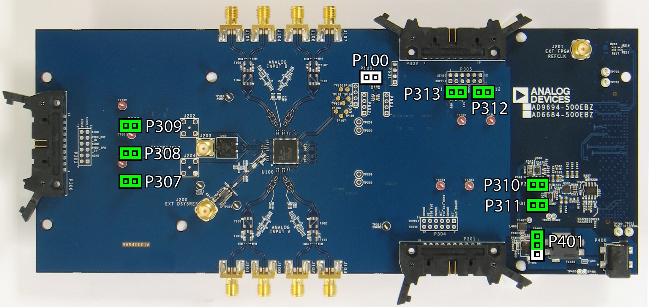
AD6684 Evaluation Board

AD6684 Evaluation Board (new version)
Typical Measurement Setup
The AD6684-500EBZ can be evaluated using the ADS7-V2EBZ FPGA data capture board. The figure below shows the AD6684-500EBZ connected to the ADS7-V2EBZ. If using the old version of the board, refer to the first image for connections, otherwise if using the new version of the board, refer to the second image.
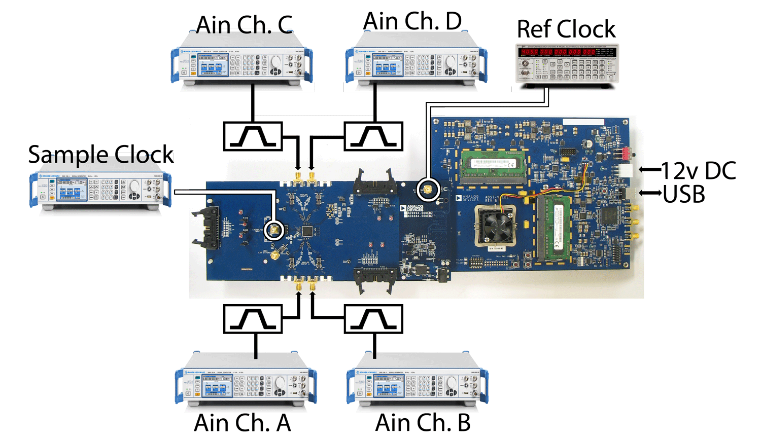
Evaluation Board Connection—AD6684-500EBZ

(New) Evaluation Board Connection—AD6684-500EBZ
Features
- Full featured evaluation board for the AD6684
- SPI interface for setup and control
- Wide band Balun driven input
- External supply powered but may also use 12V-1A and 3.3V-3A supplies from FMC
- VisualAnalog® and SPI controller software interfaces
Helpful Documents
- AD6684 Data Sheet
- ADS7-V2EBZ evaluation kit (ADS7-V2EBZ)
- AN-905 Application Note, VisualAnalog Converter Evaluation Tool Version 1.0 User Manual
- AN-878 Application Note, High Speed ADC SPI Control Software
- ADI SPI Application Note ADI Serial Control Interface Standard
- AN-835 Application Note, Understanding ADC Testing and Evaluation
Software Needed
- ACE ace
Design and Integration Files
Equipment Needed
- Analog signal source and antialiasing filter
- Sample clock source
- 12V, 6.5A switching power supply (such as the SL POWER CENB1080A1251F01 supplied with ADS7-V2EBZ/ADS7-V1EBZ)
- PC running Windows®
- USB 2.0 port
- AD6684-1000EBZ board
- ADS7-V2EBZ FPGA-based data capture kit
Getting Started
This section provides quick start procedures for using the evaluation board for AD6684.
Configuring the Board
Before using the software for testing, configure the evaluation board as follows:
- Connect the evaluation board to the ADS7-V2EBZ data capture board, as shown in the figure for the Evaluation Board Connection.
- Make sure the jumpers are placed on the evaluation board as highlighted in green in the figure AD6684 Evaluation Board.
- Connect one 12V, 6.5A switching power supply (such as the CENB1080A1251F01 supplied) to P4 on the ADS7-V2EBZ board. Connect the Standard-B USB port of the ADS7-V2EBZ board to the PC with the supplied USB cable.
- Turn on the ADS7-V2EBZ.
- If the Device Manager does not show the ADS7-V2EBZ listed, unplug all USB devices from the PC, uninstall and re-install SPIController and VisualAnalog and restart the hardware setup from step 1.
- On the ADC evaluation board, provide a clean, low jitter 1GHz clock source to connector J204 and set the amplitude to 14dBm. This is the ADC Sample Clock.
- On the ADS7-V2EBZ data capture board, provide a clean, low jitter clock source to connector J3 and set the amplitude to 10dBm. This is the Reference Clock for the gigabit transceivers in the FPGA. The REFCLK frequency can be calculated using the following empirical formulae:
bps/lane, where
(Default Nprime = 16)
- On the ADC evaluation board, use a clean signal generator with low phase noise to provide an input signal for channel A to J101. Use a shielded, RG-58, 50 Ω coaxial cable to connect the signal generator output to the ADC Evaluation Board. For best results, use a narrow-band, band-pass filter with 50 Ω terminations and an appropriate center frequency. (ADI uses TTE, Allen Avionics, and K & L band-pass filters.) If providing an input clock with a divide-by-1 setting in the AD6684 make sure the clock source has a 50% duty cycle. For optimum SNR performance use the clock divider with a divide ratio of 2 or higher to minimize the impact of the phase noise from the input clock source.
- On the ADC evaluation board, use a clean signal generator with low phase noise to provide an input signal for channel B to J102. Use a shielded, RG-58, 50 Ω coaxial cable to connect the signal generator output to the ADC Evaluation Board. For best results, use a narrow-band, band-pass filter with 50 Ω terminations and an appropriate center frequency. (ADI uses TTE, Allen Avionics, and K & L band-pass filters.)
- On the ADC evaluation board, use a clean signal generator with low phase noise to provide an input signal for channel C to J104. Use a shielded, RG-58, 50 Ω coaxial cable to connect the signal generator output to the ADC Evaluation Board. For best results, use a narrow-band, band-pass filter with 50 Ω terminations and an appropriate center frequency. (ADI uses TTE, Allen Avionics, and K & L band-pass filters.)
- On the ADC evaluation board, use a clean signal generator with low phase noise to provide an input signal for channel D to J107. Use a shielded, RG-58, 50 Ω coaxial cable to connect the signal generator output to the ADC Evaluation Board. For best results, use a narrow-band, band-pass filter with 50 Ω terminations and an appropriate center frequency. (ADI uses TTE, Allen Avionics, and K & L band-pass filters.)

Visual Analog Setup
- Click Start
All Programs
- On the VisualAnalog “New Canvas” window, select the desired AD9694 canvas. Note: The current canvases for VisualAnalog only support operating both pairs of channels in the AD6684 in the same chip operating mode with the same decimation rate. If Pair AB is in NSR mode then Pair CD must also be in NSR mode. If Pair AB is in real DDC0/DDC1 mode with a decimation rate of 2 then pair CD must also be in real DDC0/DDC1 mode with a decimation rate of 2.

Selecting the AD6684 canvas
- Next, program the FPGA in VisualAnalog by clicking into the ADC Data Capture Settings block and selecting the Capture Board tab. Use the Browse button to navigate to the ad9694_ads7v2.bin file and then click Program. The FPGA_DONE LED should illuminate on the ADS7-V1 board indicating that the FPGA has been correctly programmed.

Programming the ADS7-V2EBZ
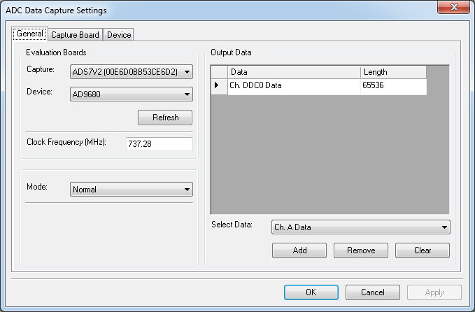
- Click the General button in the ADC Data Capture Settings block. On the General tab make sure the clock frequency is set to 2x the input clock. For example, if the input clock to the AD6684 is 368.64 MHz then set the Clock Frequency (MHz) to 737.28 MHz. The FFT capture length may be changed to 131072 (128k) or 262144 (256k) per channel. The ADS7-V2 FPGA software supports up to 2M FFT capture (1M per channel).

Changing the ADC Capture Settings
- If VisualAnalog opens with a collapsed view, click on the “Expand Display” icon (see figure 5)

Expanding Display in VA
- On the Device tab. Make sure that Enable Alternate REFCLK option is checked.
- Click OK
ACE Setup
- Click Start
- Once ACE opens the AD6684 evaluation board should appear in the Attached Hardware section.
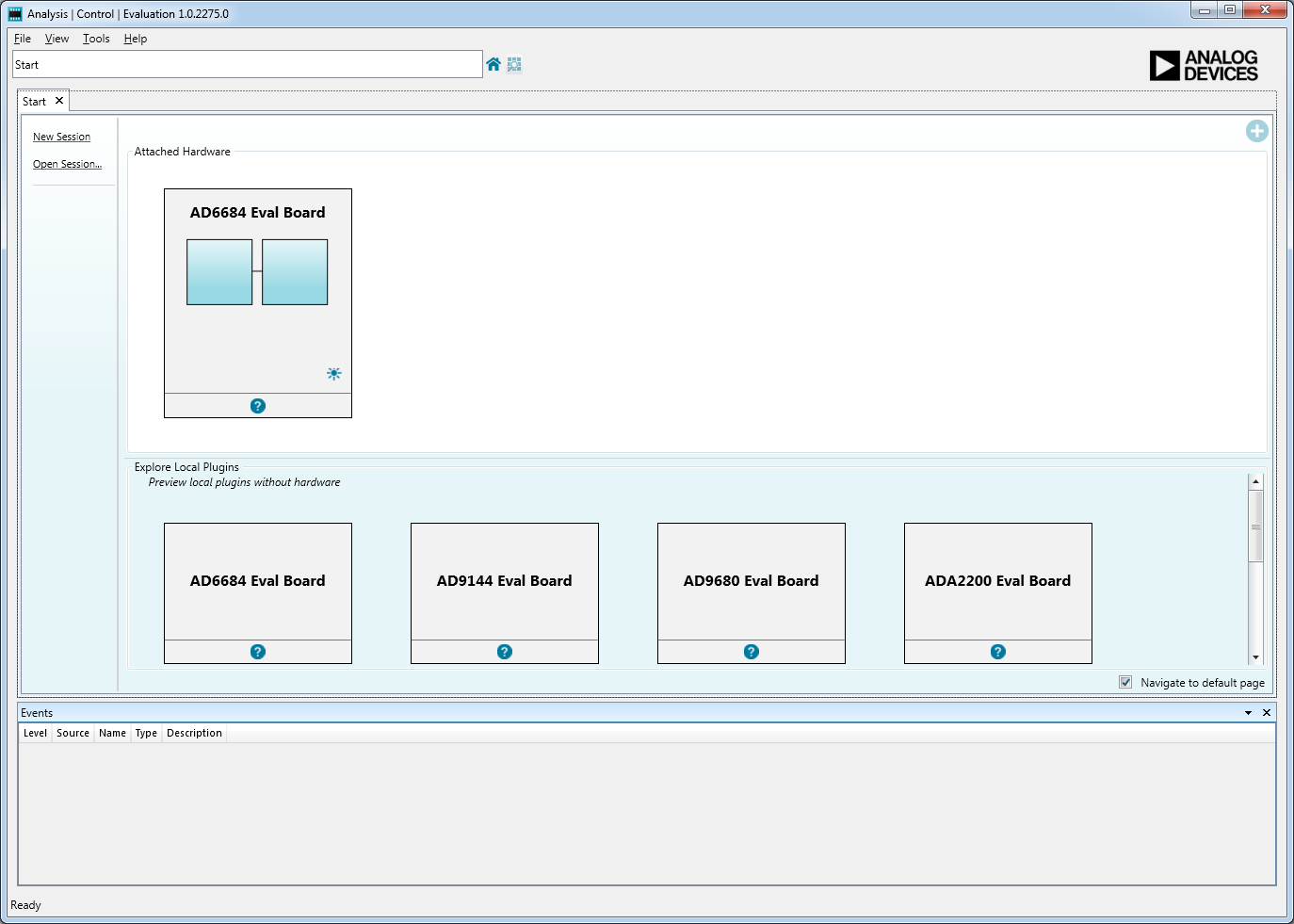
ACE Attached Hardware: AD6684
- Double click on the AD6684 Eval Board icon which will open up the Initial Configuration wizard. The default conditions for the AD6684 are NSR mode with a sample clock of 500 MHz. From here both pairs of ADC channels (Pair AB and Pair CD) can be configured simultaneously. NOTE: It is important to remember that the AD6684 functions as two dual ADCs.

ACE - AD6684 Initial Configuration Wizard
- Prior to configuring any modes in the AD6684 double click on the AD6684 icon to bring up the device view. From the device view click on the Read All icon to read the SPI settings from the device. Do this for each pair by selecting one pair at a time and then clicking the Read All icon.

ACE - AD6684 Initial Configuration Wizard
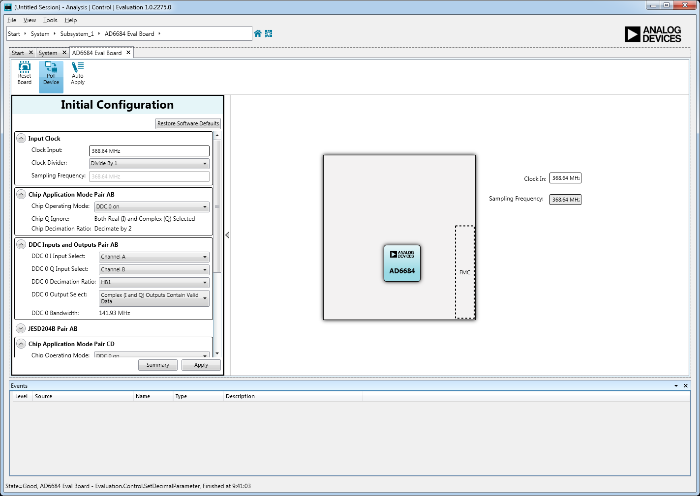
- From the the Initial Configuration Wizard the clock frequency, chip application mode (per pair), DDC inputs and outputs, and the JESD204B settings can be quickly configured. The default conditions are:
- Clock Input = 500 MHz
- Clock Divider = Divide by 1
- Chip Operating Mode = NSR Mode
- JESD204B Parameters: L.M.F = 2.2.2 ; N' = 16
- All these paramters can be seen below:

ACE - AD6684 Initial Configuration Wizard Showing JESD204B Parameters
Device Setup - NSR Mode
- The default Chip Application Mode for the AD6684-500 is NSR mode. In this example the clock frequency will be set to 368.64 MHz, the clock divider set to Divide by 1, and the chip operating mode set to NSR Mode. Once the settings have been entered, click Apply. This will configure the device with the selected settings and provide an Initial Configuration Summary which will summarize the settings that have been loaded into the AD6684 and also provide the frequency for the required FPGA reference clock.

Default Application Mode - NSR Mode
- In order to change the NSR setting for each channel, double-click on the AD6684 icon from the AD6684 Eval Board view (highlighted in the figure below).

Double-click the AD6684 Icon in the Eval Board View
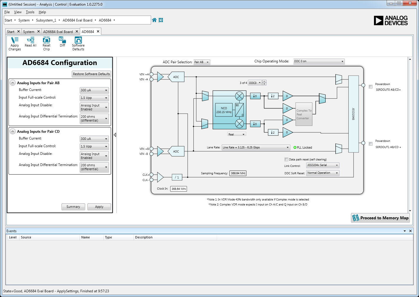
- This will bring up the AD6684 device view showing more specific settings for each pair and channel. The device view shows one pair of the AD6684 at a time. The ADC Pair Selection drop down box is used to select the current pair. To select the desired pair (Pair AB or Pair CD) select the desired pair form the drop down box. This sets the current changes to affect the select pair only. The NSR mode settings can now be configured for each channel. In this example the NSR is set to the 21% bandwidth mode with a tuning word of 58. Once the settings are configured click Apply Changes in the upper left of the device view. This will load the setting changes to the selected ADC pair and channel(s). If the settings are desired for all four channels then click the Apply button in the AD6684 Configuration window on the left of the screen. This loads the current settings to all channels in the device.

Figure 15. Pair AB - Channel A and Channel B NSR Settings
- The device view in ACE also has controls for the analog input controls. The input buffer current, input full-scale voltage, and analog input differential termination can be adjusted. The analog inputs can also be disabled from this menu.

Analog Input Control Settings
- The Memory Map View can be accessed from the AD6684 Device View. The Memory Map View can be used to individually write registers in the AD6684. Note: When writing individual registers it is imperative to first write the Pair Index register (0x0009) before any other write so that the correct ADC channel pair (Pair AB or Pair CD) is being addressed. If writing a local register, subsequently write the ADC channel index register (0x0008) so that the desired channel within the desired pair is written (Channel A/C or Channel B/D).

Memory Map View
Obtaining an FFT - NSR Mode
- The first item to configure in Visual Analog is the input clock frequency. This needs to be set to twice the frequency of the input clock. Click in the ADC Data Capture block to open the settings. In this example, 368.64 MHz is the input clock frequency so 737.28 is entered into VisualAnalog.
AD6684 FFT Data Capture Settings
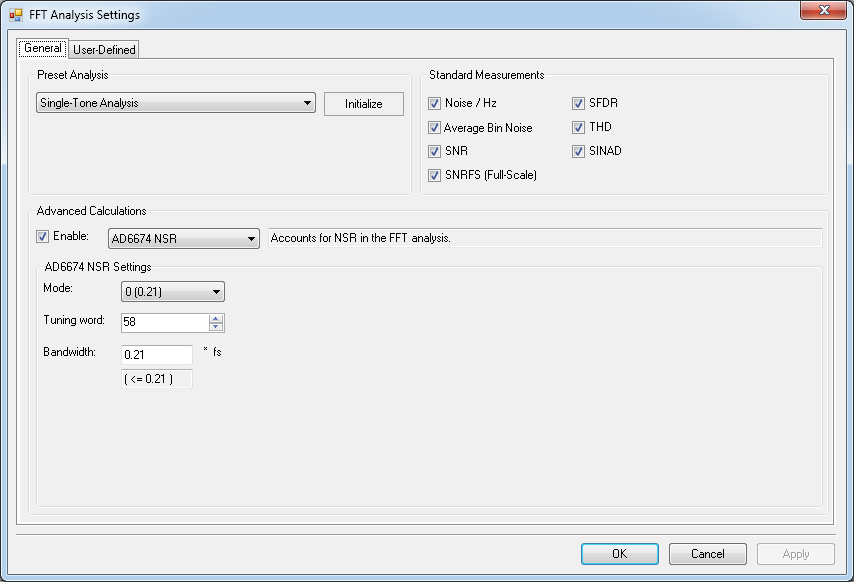
- In order to obtain an FFT with NSR enabled, Visual Analog must be configured correctly. Click on the settings button on the FFT Analysis block and configure the settings in Visual Analog to match the NSR settings that have been programmed into the AD6684. Under Advanced Calculation, click the Enable box, select AD6674 NSR, and then select the appropriate bandwidth mode and tuning word. Make sure to set the Bandwidth to match the mode. When finished, click the Apply button and then the OK button to apply the settings.
AD6684 FFT Analysis NSR Settings
- In this example, with an input clock of 368.64MHz, the output sample rate is 368.64MSPS. The default JESD204B lane configuration for the JESD204B link of each ADC Channel Pair is 2.2.2 (L.M.F). The required REFCLK frequency is 368.64 MHz (refer to step 7 in the section “Configuring the Board”).
- Click the Run button in Visual Analog and you should see the capture data similar to the plot below.

AD6684 FFT with NSR Enabled (Tuning Word = 58
- Adjust the amplitude of the input signal so that the fundamental is at the desired level. (Examine the Fund Power reading in the left panel of the VisualAnalog FFT window.) NSR imposes a ~3dB loss in the signal, but does not impact the dynamic range. A -1.0 dBFS input signal will show as -4.0 dBFS in the FFT in Visual Analog.
- To save the FFT plot do the following
- Click on the Float Form button in the FFT window
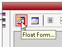
Floating the FFT window
- Click on File

Saving the FFT

Device Setup - VDR Mode
- The default Chip Application Mode for the AD6684 is NSR mode. The AD6684 settings must be changed to configure the AD6674 into VDR mode. To set up the AD6674 for VDR mode change the Chip Application Mode Variable Dynamic Range (VDR) Mode in the Initial Configuration window in the AD6684 Eval Board view in ACE and click Apply.

Set Application Mode to VDR
- The VDR mode (complex/real), bandwidth (25%/43%), and tuning word can be configured from the Device View in ACE. VDR defaults to 25% bandwidth complex mode with a tuning word of 0. In this example a real input signal is used so the tuning word and mode must be changed. See the AD6674 data sheet for more details on the available bandwidth modes and tuning words. To access the device view, double-click the AD6684 icon from the AD6684 Eval Board view which will bring up the view below. In this example VDR is set to Dual Real 25% BW Mode with the tuning word set to 6. Once the settings have been entered click Apply Changes in the upper left of the Device View. This will apply changes to the ADC Pair (Pair AB or Pair CD) selected in the Device View. To do so, set the ADC Pair Selection to the desired pair, configure the block diagram as desired and click Apply Changes in the upper left of the window. This should be done for each pair (Pair AB and Pair CD).

Pair AB: Channel A and Channel B VDR Settings
Obtaining an FFT - VDR Mode
- The first item to configure in Visual Analog is the input clock frequency. This needs to be set to twice the frequency of the input clock. Click in the ADC Data Capture block to open the settings. In this example, 368.64 MHz is the input clock frequency so 737.28 is entered into VisualAnalog.
AD6684 FFT Data Capture Settings
- In this example, with an input clock of 368.64MHz, the output sample rate is 368.64MSPS. The default JESD204B lane configuration for the JESD204B link of each ADC Channel Pair is 2.2.2 (L.M.F). The required REFCLK frequency is 368.64 MHz (refer to step 7 in the section “Configuring the Board”).
- Click the Run button in Visual Analog and you should see the capture data similar to the plot below.

AD6684 FFT with VDR Enabled (Tuning Word = 6
- Adjust the amplitude of the input signal so that the fundamental is at the desired level. (Examine the Fund Power reading in the left panel of the VisualAnalog FFT window.) Adjust the input signal to -1.0 dBFS in the FFT in Visual Analog.
- To save the FFT plot do the following
- Click on the Float Form button in the FFT window
Floating the FFT window
- Click on File
Saving the FFT

Device Setup - 1 DDC Per ADC Pair in Complex Mode with Decimation by 2 Mode
- The default Chip Application Mode for the AD6684 is NSR mode. The AD6684 settings must be changed to configure the AD6674 into DDC mode. To set up the AD6674 for DDC mode change the Chip Application Mode to DDC0 in the Initial Configuration window in the AD6684 Eval Board view in ACE and click Apply. (Note: Due to the software limitation in VisualAnalog, both ADC pairs (AB and CD) must be set to the same operating mode and same decimation rate.)
Set Application Mode to DDC0
- The DDC settings can be configured from the Device View in ACE. In this example a complex input signal is being input to the AD6684, I data is on Channel A/C and Q data is on Channel B/D. See the AD6684 data sheet for more details on the available DDC modes and decimation rates. To access the device view, double-click the AD6684 icon from the AD6684 Eval Board view which will bring up the view below. In this example DDC0 is set to complex mode with the NCO in Variable IF mode and the tuning frequency set to 230MHz (the input frequency to the AD6684 is 270.1 MHz). Once the settings have been entered click Apply Changes in the upper left of the Device View. This will apply changes to the ADC Pair (Pair AB or Pair CD) selected in the Device View.
Pair AB: Channel A and Channel B DDC0 Settings
- Once again, make sure that Pair CD has the same DDC mode as Pair AB (due to VisualAnalog software limitation). The NCO tuning and NCO mode can be different between Pair AB and Pair CD, but the pairs must both be set to complex mode or to real mode and the decimation rates must be the same. To do so, set the ADC Pair Selection to the desired pair, configure the block diagram as desired and click Apply Changes in the upper left of the window. This should be done for each pair (Pair AB and Pair CD).
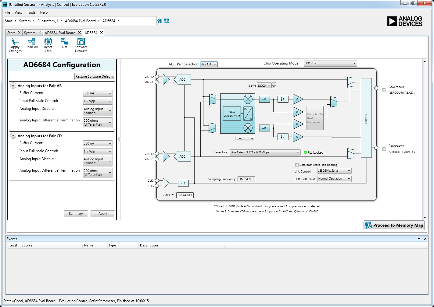
Pair CD: Channel C and Channel D DDC0 Settings
- When making changes to the DDC settings the DDC Soft Reset must be written afterwards. To do so, select DDC Held in Reset from the drop down menu in the block diagram. Then click Apply Changes in the upper left of the AD6684 Device view in ACE. Next, select Normal Operation from the drop down menu in the block diagram and then click Apply Changes once again. This process resets the DDC and then places the DDC back into normal operating mode. This must be done for each pair (Pair AB and/or Pair CD) for which DDC changes have been applied.
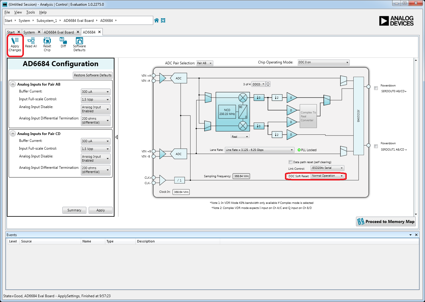
Pair AB: Channel A and Channel B DDC0 Settings with DDC Soft Reset
Obtaining an FFT - 1 DDC Per ADC Pair in Complex Mode with Decimation by 2 Mode
- The first item to configure in Visual Analog is the input clock frequency. This needs to be set to twice the frequency of the input clock. Click in the ADC Data Capture block to open the settings. In this example, 368.64 MHz is the input clock frequency so 737.28 is entered into VisualAnalog. Also, make sure that the output data is set to *Ch. DDC0 Data*.
AD6684 FFT Data Capture Settings
- In this example, with an input clock of 368.64MHz, the output sample rate is 184.32MSPS. The JESD204B lane configuration for the JESD204B link of each ADC Channel Pair is 2.4.4 (L.M.F). The required REFCLK frequency is 368.64 MHz (refer to step 7 in the section “Configuring the Board”).
- Click the Run button in Visual Analog and you should see the capture data similar to the plot below.

AD6684 FFT with DDC0 Enabled
- Adjust the amplitude of the input signal so that the fundamental is at the desired level. (Examine the Fund Power reading in the left panel of the VisualAnalog FFT window.) Adjust the input signal to -1.4 dBFS or less in the FFT in Visual Analog (this accounts for the approximately -0.4 dB loss in the DDC. Recall that the mixing process incurs a 6dB additional loss; the signal amplitude is -7.4 dBFS in this plot.
- To save the FFT plot do the following
- Click on the Float Form button in the FFT window
Floating the FFT window
- Click on File
Saving the FFT

resources/eval/ad6684-500ebz.txt · Last modified: 14 Jan 2021 05:11 by Robin Getz