 This version (30 Nov 2012 19:32) was approved by Catherine Redmond.
This is an old revision of the document!
The EVAL-AD5560EB is a full-featured evaluation board designed to allow the user to easily evaluate all features of the AD5560 DPS
The board can be controlled by two means, via the on-board connectors or via the USB port of a Windows- based PC using the AD5560 evaluation software.
The default setup is for control via the USB port.
Please refer to the AD5560 datasheet for full details on all functionality of the AD5560 device and for full details of the each of the Registers within the AD5560 .

The AD5560 is a high performance, highly integrated device power supply consisting of programmable force and measure channels. This product includes the required DAC levels to set the programmable inputs for the drive amplifier, clamping and comparator circuitry. Offset and Gain correction is included on chip for DAC functions. A number of programmable measure current ranges are available, five internal fixed ranges and two external customer selectable ranges (EXTFORCE 1 and EXTFORCE 2) which can supply currents up to 1.2A and 500mA respectively. For purposes of this evaluation board, the Rsense resistors used for the two external EXT1 and EXT2 ranges are larger than that required for a 1.2A and 500mA range respectively. This is due to the lack of cooling available for a demonstration board. The voltage range possible at this high current level is limited by headroom and the maximum power dissipation. Current ranges in excess of 1.2A or at high current and high voltage combinations may be achieved by ganging multiple DPS devices. Open drain alarm outputs are provided in the event of over-current, over-temperature or Kelvin alarm on either the sense or DUTGND lines.
The following external supplies must be provided.
Both AGND and DGND inputs are provided on the board. The AGND and DGND planes are connected at one location close to the AD5560. It is recommended not to connect the AGND and DGND elsewhere in the system to avoid ground loop problems.
Each supply is decoupled to the relevant ground plane with 10μF and 0.1μF capacitors. Each device supply pin is again decoupled with a 0.1μF capacitor to the relevant ground plane. Exposed paddle on AD5560 is internally connected to AVSS. Addition of a DUT is required for operation; please connect to gold pins or SM connections provided.
The default configuration for interfacing to the AD5560 device is via the USB interface. Access is provided to all input and output nodes via J3 in the event a user wants to drive the device by other means. In this case, remove LK9 to disconnect the on board USB circuitry. Default Link Option Setup The default setup is for control by the PC via the USB port. The default link options are listed in Table 1.
Table 1. Link Options for PC control
| Link No. | Default option | Function |
|---|---|---|
| LK1 | Inserted | Remove if USB interface is not required |
| LK2 | Inserted | Used for RESET cct |
| LK3 | Inserted | Used to connect GPO to temp Sensor |
| LK4 | Inserted | |
| LK5 | Inserted | In series with EXTMEASIL path |
| LK6 | Inserted | In series with FORCE path |
| LK7 | Inserted | In series with SENSE path |
| LK8 | Inserted | Used to connect DUTGND to AGND |
| LK11 | A | Reference selection |
| A: 5V | ||
| B: 2.5V | ||
| C: External Reference input |
The ADC is a 5V device, so gain of 0.2 (for MEASOUT) should always be selected if using ADC for measurements. If gain = 1, then LK 4 should be removed to protect the ADC (assuming that LK 4 is in position A).
The AD5560 board is flexible in that users can use any DUT at the output of each AD5560 device. Gold pin connectors allow for RDUT and CDUT connections. The range of the CDUT load should be confined to the maximum DUT capacitance as outlined in the AD5560 datasheet. (max of 160uF) The measure function may be accessed via the SMB connectors connected at the MEASOUT pin. The on board ADC can perform measurements on measured parameter, however, please remember the ADC is a 5V device, therefore, should only be used with MEASOUT GAIN = 0.2. Please remove LK4 if using MEASOUT GAIN = 1.
The AD5560 evaluation kit includes self-installing software on CR-ROM. The software is compatible with Windows 2000/NT/XP. If the setup file does not run automatically, setup.exe can be run from the CD-ROM. The evaluation software should be installed before connecting the evaluation board to the PC’s USB port to ensure that the evaluation board is correctly recognized when connected to the PC.
To launch the software, select the AD5560 submenu from the Analog Devices menu. Next, click AD5560 Evaluation Software.
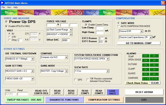
The main window of the AD5560 software looks as follows :
 This window allows user to set up all functions. Once the information is loaded to the GUI, it is loaded to the device.
The window shows a number of Tabs that allow the user to control different registers within the AD5560 and different functions on the AD5560 evaluation board, e.g. Write and Read functions of the following registers – System Control Reg, DPS Registers, DAC Registers.
 The ADC is a 5V device, so gain of 0.2 (for MEASOUT) should always be selected if using ADC for measurements. If gain = 1, then LK4 should be removed to protect the ADC.
Each of these registers require that the GREEN button be hit to load the relevant register.
The compensation selection Tabs allows access to the compensation registers to set the different compensation parameters manually or automatically. The appropriate capacitor values may be automatically selected depending on the load capacitance at the DUT. By default, the power on mode of the device (and the eval s/w) is “SAFE MODE”. Please bear this in mind when making settling time measurements.
 Each of these registers require that the GREEN button be hit to load the relevant register.
This register allows access to internal nodes within the AD5560 such as the thermal array scattered across the different portions of the die. Included on the evaluation board is a temp sensor to allow conversion of the diode voltages to temperature, see ADT7461 tab for temp sampling. The ADT7461 is an ON Semiconductor product.

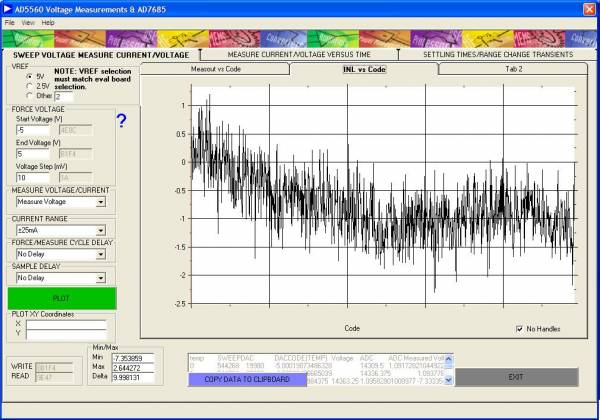
Here sweeps of current/voltage may be performed. Also measurements with respect to time (Note: time measurements will be affected by other PC operations – so may not in fact be truly representative of time).
Settling time routines and range change transients also all for analysis of the AD5560 device.
The ADC is a 5V device, so gain of 0.2 (for MEASOUT) should always be selected if using ADC for measurements.

