


This version (30 Aug 2022 19:39) was approved by Doug Mercer.The Previously approved version (02 Nov 2021 18:19) is available.
Table of Contents
Activity: Artificial Transmission Lines - ADALM1000
Objective:
The objective of this lab activity is to carry out experiments exploring the basic characteristics of wave propagation along transmission lines by examining an array of cascaded lumped-element LC sections as an effective substitute for a real transmission line.
Notes:
As in all the ALM labs we use the following terminology when referring to the connections to the ALM1000 connector and configuring the hardware. The green shaded rectangles indicate connections to the ALM1000 analog I/O connector. The analog I/O channel pins are referred to as CA and CB. When configured to force voltage / measure current –V is added as in CA-V or when configured to force current / measure voltage –I is added as in CA-I. When a channel is configured in the high impedance mode to only measure voltage –H is added as CA-H. Scope traces are similarly referred to by channel and voltage / current. Such as CA-V , CB-V for the voltage waveforms and CA-I , CB-I for the current waveforms.
Background:
Experiments for studying the basic characteristics of wave propagation along transmission lines are generally performed at frequencies in the 100's of MHz or even above 1 Ghz. These experiments usually require the measurement of the voltage or the electric field along a test section of the transmission line. From these measurements, the standing wave pattern, the phase constant, wavelength, and the VSWR of the line can be obtained. To yield the best results, the data must cover a span of frequencies that includes at least one, and preferably several, λ/2 of the standing wave, where λ represents the wavelength. This requirement can be met for a physically short line if the operational frequency is high. However, since the components and particularly the instrumentation at these frequencies are often highly specialized, a lab setup for transmission line experiments can be prohibitively expensive for a large number of students to perform such lab activities.
Since the basic characteristics of the propagation phenomena are the same for lines operating at different frequencies, an obvious low cost approach would be to utilize lines that operate at a low enough frequency where the ADALM1000 (M1k) could be used for the measurements. Although theoretically possible, this is physically impractical, since the line sections that would be required to obtain the needed data would be very long. For example, the length of the line section required to span even a single λ/2 of the standing waves at an operating frequency of 10 kHz (with a propagation velocity equal to the velocity of light in vacuum) is 15 kilometers. A practical way of getting around the need for high frequency instrumentation is to use a physical model of the transmission line rather than an actual line. The LC-section lumped element model is such an example, in which with appropriate choice of LC values, it is possible to achieve multiples of λ/2 of the standing wave with a practical number of LC sections at low frequencies.
The LC Lumped-Element Model
The idea of using a lumped-element circuit that experimentally behaves like a transmission line is based on the classical approach to analyzing the wave propagation on transmission lines. In this approach, the line is considered to be composed of an infinite number of sections, each made of discrete lumped elements R, L, C, G as depicted in LTspice schematic figure 1.

Figure 1, L-C lumped-element transmission line
The lumped LC sections can be considered as T or Pi sections. When implemented as Pi sections the first and last capacitors are equal to 1/2 the unit capacitance values. Generally at least 20 sections are needed to model a transmission line well.
We can calculate characteristic impedance of the Artificial Transmission Line. Assuming nominal component values and lossless components, the characteristic impedance of the line is found using the relationship:
The basic philosophy to choose the operating or test frequency (f) is that you don't want the equivalent electrical length (phase shift) of a single LC section to be too large. This is so you can sample the standing wave along the lumped-element transmission line with sufficient resolution. Nor do you want the phase shift of a LC section to be too small; you may not observe standing wave effects. We are looking for the optimal range here. A phase shift of 15 degrees per LC section is a good target to aim for (with the benefit of it being an integer fraction of 90 degrees).
The equation for the phase shift per section:
Now select a test frequency such that the resulting phase shift per section is 15 degrees:
Transmission Lines – General Information
A transmission line is defined as a system of conductors (wires, waveguides, coaxial cables), suitable for conducting electric power signals between two or more terminals. [McGraw-Hill Dictionary of Scientific and Technical Terms].
To send an electrical signal to a distant load, two wires are required. Since two metal conductors are, by definition, a capacitor, this implies that each section of a transmission line has some capacitance. On the other hand, as an inductor is defined essentially as a loop of wire, each section of the line also has an inductance. In reality, each “section” of the line is infinitesimally short, however, a “lumped” model of a transmission line can be constructed with discrete inductors and capacitors as shown in Figure 1. Suppose a constant DC voltage is applied to one end of the transmission line. The capacitance and inductance are what prevent the signal from traveling instantaneously. These capacitors and inductors are not components that we deliberately add to the circuit but are an inherent part of all wires that carry electrical signals.

Figure 1. Electrical equivalent of a transmission line
Voltage applied between two conductors creates an electric field between them. Equation 1 implies that the current drawn from the voltage source would be proportional to the voltage’s rate of change over time. In consonance with said equation, an instant rise in applied voltage, results in an infinite charging current. Nonetheless, the current drawn will not be infinite because of the series impedance, due to line inductance. Each wire from our pair develops a magnetic field as it carries charging current for the capacitance between the wires, dropping voltage according to equation 2. This voltage drop limits the voltage rate of change across the distributed capacitance, preventing the current from ever reaching an infinite magnitude. Thus, the wires are no longer simple conductors - they are themselves a circuit component called a transmission line, with their own characteristics. When voltage is suddenly applied, both a current wave and a voltage wave propagate along the line’s length at a significant fraction of the speed of light.
Equation 1:
where i is the instantaneous current through the capacitor;
C is the capacitance in Farads;
is the instantaneous rate of voltage change, volts per second.
Equation 2:
where v is the instantaneous voltage across the inductor;
L is the inductance in Henrys;
is the instantaneous rate of current change, amps per second.
The physical construction of a transmission line varies widely depending on the application. There are several different types of electrical transmission lines such as coaxial line (figure 4), two-wire line (figure5), parallel-plate line, strip line, microstrip line, coplanar waveguide (figure 6).
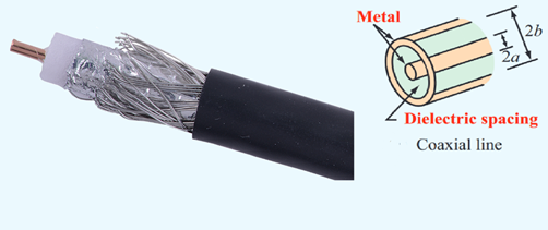
Figure 4. Coaxial line

Figure 5. Two-wire line
A common example of a 2-wire transmission line is the usual un-shielded twisted pair (UTP ethernet cable everyone is familiar with. A twisted pair that is surrounded by a solid dielectric, the line becomes a shielded pair transmission line (STP). Both cables are shown in figure 9. When using UTP transmission lines, several parameters need to be considered: attenuation (amount of loss in signal’s strength as it travels down a wire), cross-talk (unwanted coupling caused by overlapping electric and magnetic fields), near-end cross-talk (measure of level of signal coupling within a cable). A visual representation of the latter is depicted in figure 10. There are a couple of advantages to using the shielded pair cable, such as:
- Conductors are contained within in a copper braid shield, which isolates from external noise and prevents radiating and interfering with other systems.
- Conductors are balanced to ground, thus capacitance between wires is uniform throughout the length of the cable.
Characteristic Impedance
Characteristic/ natural impedance refers to the equivalent resistance of a transmission line if it were infinitely long, owing to distributed capacitance and inductance, as the voltage and current waves travel along its length at a propagation velocity equal to some large fraction of the speed of light. Suppose the spacing between the two conductors is expanded. Under this condition, the distributed capacitance will decrease, while the distributed inductance will increase, as there is less cancellation between two opposing magnetic fields. Naturally, by bringing the capacitor plates (the two conductors) closer together, the antagonistic effect is obtained: increased parallel capacitance and decreased series inductance. Hence, one can note that the characteristic impedance of a transmission line increases as there is greater space between conductors. To calculate the natural impedance of a given transmission line, with known parameters, the following formula shown in equation 3 is to be used. This shows that characteristic impedance is purely a function of the capacitance and inductance distributed along the lines length and it would exist even if the dielectric were perfect (infinite parallel resistance) and the wires superconducting (zero series resistance).
Equation 3:
where characteristic impedance of line;
L – inductance per unit length of line;
C – capacitance per unit length of line.
Give the formulas for characteristic Z of UTP and co-axial cable, based on geometery - these should be easy to find, with figures
The inductance and capacitance, and hence the characteristic impedance, are functions of the geometry. The characteristic impedance of a UTP transmission line is shown in Formula X, and the characteristic impedance of a coaxial transmission line is shown in Formula Y…
Formula X
Formula Y
Incident and Reflected Waves
A signal which travels from the source-end of the transmission line to the load-end, is called an incident wave, while a wave which propagates in the opposite direction is defined as a reflected wave. Leaving the end of a transmission line open-circuited (unconnected), results in a pile-up of electric charge carriers at the line’s end, as the incident current wave propagating along the line cannot flow where there is no continuing path. When this electric charge carriers propagates back as a reflected wave, current at the source ceases, and the line becomes a simple open circuit. A similar event occurs when the line’s end is short-circuited: the voltage wave front is reflected to the source, as it reaches the end of the line, since voltage cannot exist between two electrically common points. As the reflected wave arrives at the source-end, the source views the entire transmission line as a short-circuit. Reflections may also appear when connecting two transmission lines, whose characteristic impedance differ. When dealing with signal transmission, it is important to state that the ideal situation would be for the entirety of the original signal’s energy to travel from source to load, and then be completely absorbed or dissipated by the load, with the maximum signal-to-noise ratio. It is then obvious that both loss along the line and reflected waves are undesirable.
Reflections may be avoided, if the load’s impedance matches the characteristic impedance of the transmission line, making the line seem infinitely long, as far as the source is concerned. This is due to a resistor’s ability to continuously dissipate energy, just as an infinitely long transmission line would eternally absorb energy. Should the source’s impedance be exactly equal to the line’s, a reflected wave, which reaches the source, would be dissipated entirely. However, if these two quantities do not match, the wave is partially re-reflected to the load end of the line, as another incident wave.
Figure 11: Free end (left) and fixed end (right) reflection of incident wave
Wave- and Transmission Lines’ Length
The length of a transmission line is admitted short when the propagation effects are much quicker than the conducted signal’s period. In opposition, a line is considered electrically long when the propagation time is a large fraction or a multiple of the signal period. To approximate, when the signal waveform completes at least a quarter-cycle before the incident wave reaches the line’s end, the transmission line is defined as long. When dealing with a short line, the terminating (load) impedance dominates circuit behavior, as the source sees nothing but the load’s impedance. On the other hand, a long line’s own characteristic impedance dictates circuit performance.
Wavelength can be defined as the expression of distance traveled by a signal along a transmission line in relation to its source frequency. A simple formula, known as the wave relation (marked as equation 4), is used to solve most problems in this area, obeying the scheme shown in figure 12.
Equation 4:
where v is the velocity of propagation, f is the signal frequency, and λ is the wavelength.
Figure 12: Problem solving scheme
Due to the high speed with which the signal travels, in order to measure transmission line parameters, very fast test equipment is required. Such equipment includes radio-frequency generators, pulse generators, fast oscilloscopes, and time-domain reflectometers.
Standing Waves and Resonance
Let there be a transmission line with a mismatch in impedance between the line and the load. Reflections which occur will mix with the oncoming incident waveform, producing standing (stationary) waves. A standing wave is, actually, the only voltage along the line, as it is obtained by adding the reflected wave to the incident wave, as shown in figure 14. Though it oscillates in instantaneous magnitude, a standing wave does not propagate along the wire’s length. When analyzing standing waves, two categories of points arise: a node – a point on a standing wave where the amplitude is minimum, and an antinode – a point on a standing wave where the amplitude is maximum. Nodes remain fixed, while the position of the antinodes may vary. The standing wave pattern is given by alternating the nodal and anti-nodal positions. A method of expressing the magnitude of the effect that standing waves have on our transmission line is a as a ratio of maximum amplitude (antinode) to minimum amplitude(node), for either voltage or current. This is known as the standing wave ratio (SWR). A perfectly terminated transmission line implies SWR=1. Certain frequency values will determine a correlation between the nodes and antinodes, which results in resonance. Should the maximum values of amplitude of the standing waves be exceedingly high, the transmission line may be subject to deterioration. Voltage antinodes may loosen the insulation between conductors, while current antinodes may cause excess heat in the conductors.
Simulation
Below is an LTspice simulation schematic of both an ideal transmission line model and modeled as the lumped L-C equivalent circuit.

Additional Background Material
Even more detailed background material on transmission lines can be found in this ADALM2000 Lab Activity.
Materials:
ADALM1000 hardware module
20 inductors with values in the range of 47 uH to 150 uH
21 capacitors with values in the range of 6.8 nF to 100 nF
2 resistors with values in the range of 27 Ω to 56 Ω
1 CD4052 or 74HC4052 4:1 analog CMOS multiplexer (optional)
Looking at the standing wave pattern along an artificial lumped LC transmission line.
While it is potentially possible to construct a 20 section LC transmission line model on a solderless breadboard using thru-hole devices it is difficult and can be problematic to get the expected results. Constructing the transmission line model on a more compact PC board using surface mount components is a more reliable solution and produces better results.
The experiment PC board shown figure 2 is from the education tools on the ADI GitHub repository and has 20 sections. The specific board shown is populated with 100 uH surface mount inductors and 47 nF thru-hole capacitors. The board can be populated with either SMD or thru-hole components. The above L and C values give a characteristic line impedance of close to 50 ohms so 47 ohm source and termination resistors are used.

Figure 2, Lumped LC transmission line experiment board.
Male pin headers around the board provide connection points at each tap along the line to measure the delayed waveforms. The M1k has only two “Scope” inputs so measuring and displaying the waveforms at all 21 taps can be tedious. The ALICE desktop software has an option to employ an external 4:1 analog CMOS mux (such as a CD4052) to expand the number of signals that can be displayed using the CH B input to 4. This is a simple enough circuit to build on a solderless breadboard but an auxiliary PC board that plugs into the 8 pin analog connector of the M1k is also available from the education tools on the ADI GitHub repository. Figure 3 shows the M1k with the mux board connected to one of the LC transmission line boards at 5 different taps more or less evenly spaced along the line.

Figure 3, M1k plus Mux accessory board connected to lumped LC transmission line.
The screen shot in figure 4 shows the results using the Phase Analyzer Tool in the ALICE desktop. The green reference phase (always CH A) is the first tap. The other four are more or less evenly spaced along the line with the last input, the yellow vector, on the final end tap. The line was terminated with a resistor equal to the line impedance (no reflections). The Frequency of the input sinewave is set to about 6 KHz which seems to be about where 1/4 the wavelength is equal to the line length (90 degree phase shift at the final tap).

Figure 4, M1k plus Mux accessory board connected to lumped LC transmission line.
It is also possible to plot the Channel A current vector at the same time which shows how “resistive” (or not) the input port of the line looks. In figure 5 the transmission line input current phase and amplitude with the end shorted is plotted along with the voltage amplitude and phase for the first 5 taps.

Figure 5, Plotting the transmission line input current phase and amplitude (end shorted).
One of the features in the Phase Analyzer is the ability to save any or all of the amplitude and phase values to a comma separated values (csv) file. The Save Data button under the File menu will ask for a file name and then append the currently selected data to the file if it exists or create a new file if not. If the Append option is checked the data will be appended to the last file name entered (without requesting a new file name). Once a list of vector values has been saved to a file the vectors can be plotted on the grid using the Plot From File button.

To gather data for the entire transmission line, the four Mux inputs are moved along the taps in groups of four keeping CH A connected to the first tap as the reference phase. The values for three line conditions, terminated, open and shorted, were saved to files. It is then possible to plot the values from the saved files back onto the grid. Figure 6 plots the amplitude and phase vectors for all 21 taps of the terminated line.

Figure 6, Phasor plot for all taps, terminated line.
The csv file was then loaded into Excel and after some minor editing a plot of the amplitude vs tap position is made as shown in figure 7.

Figure 7, Plot of amplitude vs tap position for Terminated line.
The same process is repeated for the open line case as shown in figure 8.

Figure 8, Phasor plot for all taps, open line.

Figure 9, Plot of amplitude vs tap position for open line.
For the open line condition in figure 9, we can clearly see the standing wave pattern along the taps of the line with peaks at the beginning middle and end of the line as you would expect. The same process is repeated for the shorted line case, figure 10.

Figure 10, Phasor plot for all taps, shorted line.

Figure 11, Plot of amplitude vs tap position for shorted line.
For the shorted line condition in figure 11, we can clearly see the different standing wave pattern along the taps of the line with nulls at the beginning middle and end of the line as you would expect.
Other Transmission Line Characteristics
The ALICE Impedance Analyzer Tool and Bode Plotting Tool can be used to measure other characteristics of the artificial transmission line input and output ports vs frequency.
Appendix: Solder-less breadboard build
It is possible to get passable results when constructing an artificial transmission line on a solder-less breadboard. But only if done carefully. Using only components with short leads that fit snugly and tight to the breadboard will give adequate results. The components must be arranged such that very few jumpers are required and they also are fitted tight to the breadboard (from the ADALP2000 parts kit) as shown in figure A1.

Figure A1, M1k plus Mux accessory board connected to breadboard transmission line.
20 Axial lead 560 uH inductors were used with their leads cut short and bent to fit into 0.4” spacing on the breadboard. These particular inductors have heavier gauge leads that fit snugly in the breadboard making good contact. 23 47 nF Mylar capacitors were used. These particular capacitors have short heavier gauge leads that also fit tightly to the breadboard making solid contact.
The combination of 560 uH and 47 nF values gives a calculated line impedance of 110 ohms. The DC series resistance of each inductor is 6.5 ohms. The total series resistance is nearly the same as the line impedance and results in significant attenuation along the line. The delay of the line was measured at approximately 100uSec. The standing wave pattern along the line was tested with the same three terminated, open and shorted conditions. The plot of amplitude, at 9765 Hz, vs tap position for the three conditions is shown in figure A2.

Figure A2, Plot of amplitude vs tap position for breadboard line.
Appendix: External Analog Multiplexer
The use of just about any generic analog multiplexer integrated circuit is possible with the ADALM1000 to extend the number of voltage input channels. Here are two examples. The first example uses the common CD4052 (or 74HC4052) dual 4:1 analog switch. In addition the PDIP versions of the MAX4618 and MAX4582 are pin compatible with the industry-standard 74HC4052.
While the mux can be simply included on your solderless breadboard alongside the rest of the experiment it is often much more convenient to have it on an accessory plug in board as shown. Information and design files for this accessory board can be found in this web page and on GitHub, M1k Accessory Board, Dual 4:1 Analog Input Multiplexer.

Figure A1, M1k Mux accessory board

Figure A2, M1k Mux accessory board attached to poly phase filter and an M1k
Another analog mux board is this one based on the 16:1 CD74HC4067 from SparkFun Analog/Digital MUX Breakout. It does not come with header connectors so they would need to be added. The pins on the connector do not line up with the M1k connectors so male to male jumpers would be needed as shown in the next figure.

Figure A3, SparkFun Analog Mux break-out board

Figure A4, CD4067 mux break out board attached to poly phase filter and an M1k
A similar 8:1 analog multiplexer break-out board using the 74HC4051 circuit is also available from SparkFun.
For Further Reading:
Artificial transmission line, from Wikipedia,
Artificial (lumped element) Transmission Line
Telegrapher's equations
Bounce Diagrams
Return to Lab Activity Table of Contents.
university/courses/alm1k/alm-lc-atline.txt · Last modified: 30 Aug 2022 19:39 by Doug Mercer