


This version is outdated by a newer approved version. This version (05 Nov 2021 14:55) was approved by Doug Mercer.The Previously approved version (14 Jan 2021 05:38) is available.
This version (05 Nov 2021 14:55) was approved by Doug Mercer.The Previously approved version (14 Jan 2021 05:38) is available.This is an old revision of the document!
Table of Contents
Activity: DC-DC Converters I - ADALM1000
Objective:
The object of this activity is to explore an inductor based circuit which can produce an output voltage which is higher than the supplied voltage. This class of circuits are referred to as DC to DC converters or boost regulators.
Notes:
As in all the ALM labs we use the following terminology when referring to the connections to the M1000 connector and configuring the hardware. The green shaded rectangles indicate connections to the M1000 analog I/O connector. The analog I/O channel pins are referred to as CA and CB. When configured to force voltage / measure current -V is added as in CA-V or when configured to force current / measure voltage -I is added as in CA-I. When a channel is configured in the high impedance mode to only measure voltage -H is added as CA-H.
Scope traces are similarly referred to by channel and voltage / current. Such as CA-V , CB-V for the voltage waveforms and CA-I , CB-I for the current waveforms.
The circuits used in this Lab activity while generally low current can produce voltages beyond the 0 to 5 V analog input range of the ALM1000. Input voltage divider techniques as discussed in the document on ALM1000 analog inputs will be required. Refer to the document and construct and use input dividers before preforming any of these experiments with the ALM1000.
Background Basics:
When the current flowing in an inductor is quickly interrupted a large voltage spike is observed across the inductor. This large voltage spike can in fact be useful in some cases. One example is the DC to DC boost converter, which is a circuit that can create a larger DC voltage from a smaller one with very high efficiency. The basic idea is to combine an inductive spike generator with a rectifier circuit, as shown in figure 1. Whenever the transistor is abruptly turned off the voltage at the drain spikes up, the diode D1 is forward biased and current will flow from the inductor to charge up the high capacitance storage capacitor C2. When the drain voltage subsequently drops below the voltage on the capacitor, the diode is reverse biased and the output voltage remains constant. Just as in the chapter on AC power supplies, the output capacitor must be sized appropriately to minimize the ripple relating to the current flowing in the load. We will just use a small capacitor here and therefore the circuit will not be able to source a large output current. The following simulation activity will provide more insight into how a Boost configuration operates:
Activity 1: An Ideal* Open-Loop Boost Converter Simulation
* (This exercise will use the term “ideal” extensively. A more accurate term would be “almost ideal” - LTspice requires finite numbers in certain locations - switch on and off resistances can't be zero or infinity, so we're using values small enough and large enough to have negligible impact on the results.)
Open the OL_Boost_concept_ideal_sw.asc LTSpice file. Notice the differences between this circuit and the buck converter:
- One side of the inductor is connected directly to the input supply.
- The switches are rearranged, with S1 allowing the input supply to be connected directly across the inductor, and S2 allowing the inductor to be connected or disconnected from the output.
As with the buck basics lab, let's keep two things in mind at all times:
- Current through an inductor can't change instantaneously
- The DC voltage across an inductor is zero
The figure below shows the “charge” state of the circuit’s operation, where S1 is closed and S2 is open.

Figure 2. Boost Converter Charge
When S1 closes, the left-hand side of the inductor is connected to the 5V supply, and the right-hand side is connected to ground. This means the voltage across the inductor is simply the 5V supply. This “charges” the inductor with a current that ramps up with a positive slope of:
Note: The polarity of the voltage across the inductor is arbitrary, we're using the convention that a positive voltage is one that causes an increase in energy stored in the inductor.
The next figure shows the other state, with S1 open and S2 closed.
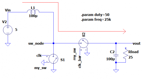
Figure 3. Boost Converter Discharge
When S2 closes, the left-hand side of inductor L1 is still connected to Vin, while the right-hand side is now connected to Vout. The current through L1 is now flowing to the output, and decreasing with a negative slope of:
Similar to the buck converter basics activity 1 the “freq” and “duty” parameters set the frequency of the switching to 25kHz and the duty cycle of the voltages imposed on this switch node (sw_node) to 50%. That is, the righthand side of the inductor spends half of the time connected to ground (charging phase), and half of the time connected to the output (discharging phase). Run the simulation, and probe sw_node, Vout, and the current through inductor L1. Zoom in toward the end of the run after the startup transient damps out (after 8ms). (You can right-click, Auto range y-axis to line up the two waveforms.)
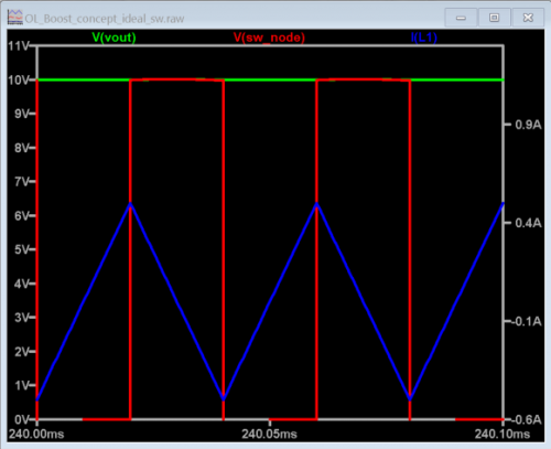
Figure 4. Boost Converter Switch Node, inductor current, and Output
Observe the peak and valley of the waveform I(L1) (green waveform), noting the current ripple. Using the cursors from peak to peak, we can observe that the inductor is charging and discharging linearly (with the period of 1/25kHz, or 40us, with a duty cycle of 50% making ts1 and ts2 20us each).
The output voltage is almost exactly 10V - double the input voltage - with a small ripple imposed. Verify that the previously solved equations are true, using the cursors to measure the inductor current waveforms.
For the “charge” phase:
And for the “discharge” phase:
Revisiting the concept of zero DC across an inductor, how can we find the output voltage of a boost converter knowing the input voltage, frequency, and duty cycle? “Zero DC across an inductor” means that over a long period of time, the average volt-second product is zero. Thus:
Where tS1 is the time that S1 is closed, tS2 is the time that S2 is closed. Rearranging, we see that:
Note that
is the duty cycle of the switch node, we can rewrite the expression for VOUT as a function of duty cycle:
Since our duty cycle is based off ts1 and ts2, and the duty cycle is always between 0% and 100%, the above equation demonstrates that the average output voltage is always equal or larger than the input voltage, a basic property of a boost converter, and at a 50% duty cycle, the output voltage is double the input voltage.
Now change the duty cycle in the simulation and re-run. The following are screenshots show the output voltage at 20% duty cycle(expected output of 6.25V) and 80% duty cycle(expected output of 25V).

Figure 5. Boost converter output with a duty cycle of 20%

Figure 6. Boost converter output with a duty cycle of 80%
Can you boost to an arbitrarily high voltage? See Appendix: “Extreme Boosting” to find out.
Load Regulation
So far we've operated the boost circuit unloaded. In this condition, the duty cycle to boost factor relationships held true, but what happens if you start to draw current from the output (as you would in a practical circuit - after all, a power supply exists to power stuff!) Furthermore, consider the boost converter's output switch (S2). If we look at the current waveform and the voltage waveform of the unloaded circuit, we see that for part of the cycle, the inductor current goes negative, and when this occurs, the output voltage is ramping DOWN! This seems counterproductive for a boost converter, doesn't it? This mode of operation has a name - “Forced Continuous Conduction Mode”. It is forced because the switches always impose a voltage across the inductor, so its current is always either ramping up or down.
Next, connect the 25 ohm load resistor to the output node (drawing an average current of 0.4 amps from the 10V output). Note that the impact on the output voltage is minimal, and the inductor current is still ramping up and down with the same peak-to-peak ripple, however the current is now always positive (flowing from input to output, according to our convention.)

Figure 7. Ideal Boost Converter with 25Ω load
But are we still FORCING this circuit to conduct continuously? We'll find out shortly…
Materials:
ADALM1000 hardware module
Solder-less breadboard and jumper wire kit
1 - 2N3904 small signal NPN transistor
1 - ZVN2110A NMOS FET (2N7000 or power FET device such as IRF510)
Various resistors
1 - 1mH inductor
Various capacitors
1 - HPH1-1400L (Coilcraft Hexapath inductor)
2 - rectifier diodes (1N4001, 1N3064)
Additional Equipment:
Small handheld DMM
battery holder for 2 AA cells to provide 3V
Simple inductor and switch DC/DC Converter:
Build the circuit in figure 1 on your solder-less breadboard. Note that in this inductor based DC to DC converter the spikes of current needed may exceed the limits of the onboard +5V supply causing it to shut down. You should use a standalone wall powered bench supply or batteries. You can use a 1N4001 or a 1N3064 for the rectifier diode. Start with a load resistance of 100 kΩ and a switching frequency of 2 kHz which can be supplied by the channel A voltage generator CA-V. What is the DC voltage of the “boosted” output? Record the value for your lab report.

Figure 1 Simple DC to DC converter
Now increase the frequency to 4, 6 and 8 KHz. Measure and record the output voltage again. Explain why it has changed? One advantage we have here is that we can control the time period between the peaks of the signal going into the rectifier; in the power supply lab, we were stuck with a 60 Hz source.
Next decrease the load resistance to 10 kΩ and again measure and record the output voltage.
Clearly what is needed if we want a constant output voltage is some active regulation to keep the voltage constant when the load resistance changes. A larger output capacitance to filter out the ripple would be a good addition as well. There are a few simple ways to implement the active regulation, and indeed there are a number of other interesting design considerations for DC to DC boost converters that you can read about if you are interested, but our goal here is really just to illustrate the concept, so the circuit shown in figure 1 is not optimal in any practical sense. With more careful design, boost converters can drive a much larger output current at very high conversion efficiency (very little wasted power).
Gated Oscillator Integrated Circuit
Note that the DC to DC converter in figure 1 requires a square-wave generator to drive it. Ordinarily this square-wave generator is part of the circuit and also powered by the input supply, so that the conversion circuit is self-contained. A place to perhaps obtain a gated oscillator integrated circuit with a built in NMOS FET switch is a solar powered garden stake light such as shown in figure 2:

Figure 2, Solar powered garden light
Inside these lights is a DC-DC boost LED diver integrated circuit which increases the voltage of a 1.2 V rechargeable AAA battery to the approximately 3 V needed to dive the white LED. Many versions contain a four pin voltage boosting integrated circuit marked YX8018. Some other versions contain a functionally equivalent 4 pin IC mounted under black epoxy directly on the PC board. Either version can be used in this Lab. The complete circuit is shown in figure 3.

Figure 3, solar garden light circuit
The YX8018 comes in a 4 pin transistor style TO-94 package and the pin configuration and block diagram is shown in figure 4. A low voltage near the negative battery voltage (GND) on the CE input of the YX8018 gates off the oscillator. A high voltage near the positive battery voltage (VDD) conversely gates the oscillator on. Other versions of these LED drivers may work opposite so be sure to check your particular IC confirm how the CE control input operates.

Figure 4 YX8018 package pinout
The gated oscillator in the YX8018 runs at approximately 200 KHz driving an open drain NMOS switch ( output on LX pin1 ). The circuit pulses the inductor to step up the voltage to drive the LED.
To reduce the component count the application of the YX8108 chip is rather ingenious. They use the internal ESD diode between the CE ( chip enable ) input and ground for charging the NiCd cell from the solar panel, but also use the voltage ( or lack thereof ) from the solar panel to detect when it is dark enough to turn the LED on. The CE input includes a small pull-up current (30 uA with 1.25 volts on VDD). This small current will pull pin 3 high gating on the oscillator if the solar panel is not generating more than 30 uA of current.
We can learn more about inductor based DC-DC Converters by building various configurations around the YX8018 chip. Some of the following circuits are from the figures in the datasheet of the YX8018, others are extensions based on conventional DC-DC converter techniques. Note that in most of these examples we leave the CE pin floating for continuous operation.
In figure 2 the current pulses from the inductor return to the battery through the LED to the ground side of the battery. We can also connect the LED across the inductor so that the inductor current returns directly to the inductor as shown in figure 5.

Figure 5 Alternate way to connect the LED
The basic configurations in figures 3 and 5 drive the LED with pulses of current at the oscillator frequency. This is fine because the frequency is way above anything the eye can perceive as flicker. These pulses can be rectified and filtered into a DC voltage to drive the LED as shown in figure 6. Rectifying diode D1 can be a standard diode such as a 1N914 but a more efficient choice for these low voltages would be a Schottky diode. At these high frequencies, filter capacitor C1 does not need to be very large, a 0.1uF or 1.0uF value will work well.

Figure 6 Adding DC rectifier to the boosted output.
Applying a pulse width modulated square wave using one of the generator output channels from the ALM1000 to drive the CE input could serve as a way to change the brightness of the LED.
By adding another diode and capacitor negative output voltages can be generated as shown in figure 7. A negative voltage is not necessarily needed to drive the LED. This is more a demonstration of how DC-DC converters can also generate negative voltages from positive voltages. Capacitor C1 and diode D1 level shift the positive peaks of the voltage waveform at pin 1 and clamp the voltage seen at the junction of D1 and D2 to a diode above ground. This now negative going waveform is rectified by D2and filtered by C2. Again a more efficient design would be to use Schottky diodes.

Figure 7 Negative voltage generator.
The YX8018 datasheet includes a table listing the output current at a VDD of 1.25 V for different inductor values, reproduced here.
| L1 Inductor value | Output Current |
|---|---|
| 560uH | 3.0mA |
| 220uH | 7.0mA |
| 150uH | 10mA |
| 82uH | 15mA |
| 68uH | 21mA |
| 47uH | 30mA |
Another option is to replace the simple inductor with a transformer. The Coilcraft Hexapath 6 winding HPH1-1400L has a winding inductance of 200 uH so it falls in the range of values listed in the table. In figure 6 the HPH1-1400L is configured as a 1:5 step up transformer and the circuit can deliver 1 mA of current to a 15 KΩ load resistor ( or 15 V DC ).

Figure 8 Transformer DC-DC booster delivers 1 mA at 15 V.
Adding active regulation:
Adding a voltage comparator to drive the CE input with feedback from the boosted output adds regulation to the circuit. A regulation scheme which includes a fixed voltage reference and an error amplifier is more complex but a simpler version can be made by adding just a couple of resistors and an NPN transistor to figure 6 which demonstrates the concept. Figure 9 shows the additional circuitry.

Figure 9 Adding negative feedback regulates the output voltage.
The regulated output voltage will be N times the VBE of Q1 (a 2N3904 works well). The multiplication factor N is set by the resistor divider ratio. Using the 10 K? potentiometer and the resistor values shown the output should be adjustable to a range of voltages around +5 V. The load regulation is fairly good up to the maximum current based on the chosen value for L1 however, the temperature stability will be rather poor because of the strong negative TC of VBE.
For Further Reading:
http://en.wikipedia.org/wiki/Boost_converter
Return to Lab Activity Table of Contents
university/courses/alm1k/alm-lab-15.1636120524.txt.gz · Last modified: 05 Nov 2021 14:55 by Doug Mercer