


This version (27 Jan 2022 18:26) was approved by Pablo del Corro.The Previously approved version (09 Sep 2021 00:01) is available.
Table of Contents
-- ADXL367 Quick Start User Guide --
Device Overview
The ADXL367 is a 3-axis, Ultra Low Power accelerometer, capable of sensing a up to full-scale range of ±8 g, with 14 bits resolution. This sensor consumes only 0.8 μA at a 100 Hz output data rate and 160 nA when in motion-triggered wake-up mode, with a voltage supply range from 1.1V to 3.6V, enabling single-cell battery operation.
The ADXL367 is a second generation of Analog Devices' ultra low power accelerometers, replacing our own ADXL362 and enabling 24/7 motion sensing for vast range of markets and applications, without compromising performance at all.

Differences and improvements of ADXL367 compared to ADXL362
The following table highlights the key performance metrics and features similarities and differences between these two accelerometers:

Main differences in terms of package and size are highlighted in orange, and performance and features improvements are highlighted in green.
ADXL367 has better resolution, lower current consumption and noise density, while also providing a wider supply range and extra digital features compared to the ADXL362.
Sensor Orientation
The ADXL367 reports positive acceleration when it is accelerated in the direction of the sensing axes shown in figure below.

Gravity, which is a constant +1 g acceleration force, also factors into the overall response of the ADXL367. The figure below shows the output response to gravity.

Recommended Application circuit
Dual power supply (Vs ≠ Vddio)
It is also recommended that VS and VDDIO be separate supplies to minimize digital clocking noise on the VS supply. Below is the recommended power supply decoupling schematic. If additional decoupling is necessary, place a resistor or ferrite bead, no larger than 100 Ω, in series with VS. Additionally, increasing the bypass capacitance on VS to a 1 μF tantalum capacitor in parallel with a 0.1 μF ceramic capacitor may also improve noise. Note that increasing the resistor and capacitor values will increase your RC time constant. This will affect the reset time of the device. This means you will need a longer reset time. Turn-on time may also be slower.

Single power supply (Vs = Vddio)
For single supply condition, the recommended decoupling schematics is shown below.

Serial Communication Configuration
SPI:
The ADXL367 communicates via a 4-wire SPI or I2C and operates as a slave. The MISO pin is in a high impedance state, held by a bus keeper, except when the ADXL367 is sending read data (to conserve bus power).
Wire the ADXL367 for SPI communication as shown in the connection diagram in Figure 38. The recommended SPI clock speeds are 1 MHz to 8 MHz, with 12 pF maximum loading.
The SPI timing scheme follows with clock polarity low (CPOL=0) and clock phase zero (CPHA=0).
Refer to the datasheet for timing specifications.

SPI Commands
The SPI port uses a multibyte structure wherein the first byte is a command. The ADXL367 command set is
- 0x0A: write register
- 0x0B: read register
- 0x0D: read FIFO
I2C:
The figure below shows the recommended electrical connection for I2C communications (ASEL pin connected to VDD I/O). The 7-bit I2C address for the device is 0x53, followed by the R/W bit. The user can select an alternate I2C address by connecting the ASEL pin to the ground, in which case the 7-bit I2C address is 0x1D, followed by the R/W bit.

External pull-up resistors, Rp, are necessary for proper I2C operation. Refer to the UM10204 I2 C-Bus Specification and User Manual, Rev. 6—4 April 2014, chapter 7, section 1 (Pull-up resistor sizing) when selecting pull-up resistor values.
The ADXL367 support standard (100 kHz) and fast (400 kHz) data transfer modes. Refer to the ADXL367 datasheet for timing specifications and a command sequence.
Basic Initialization
When powered, the ADXL367 is in Standby mode by default. It is recommended to confirm the validity of a communication sequence by reading the DEVID_AD register (Address 0x00). The DEVID_AD register is read-only, and contains the value 0xAD. If the data read from DEVID is not 0xAD, it indicates that either the physical connection or command sequence is incorrect.
The flow diagram bellow shows an example of the simplest initialization routine for synchronous data acquisition of N samples at the default Output Data Rate (ODR) of 100Hz and +/-8g range, using DATA_READY interrupt mapped to INT1 pin:
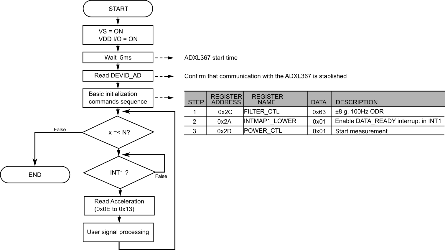
The DATA_READY interrupt signal indicates that all three axes of acceleration data have been updated in the data registers. It is latched high when new data is ready. Use the low-to-high transition to trigger action on an interrupt service routine. Data is read from the XDATA_H, XDATA_L, YDATA_H, YDATA_L, ZDATA_H, and ZDATA_L registers (0x0E to 0x13). To ensure data coherency, use multibyte reads to retrieve data from the ADXL367. The DATA_READY interrupt is cleared once the data is read.
Always make that the ADXL367 is in Standby mode first before configuring any register.
Data Formatting
The ADXL367 resolution is 14bits and its registers length is 8 bits. Thus the acceleration data of each axis is stored in two registers. For example, for X-axis XDATA_L is the low byte register and XDATA_H is the high byte register. Data is formatted as Left-Justified, so the two less significant bits of XDATA_L are not of interest. Once acceleration data is acquired from data registers, the user must reconstruct the data as a 16-bits word length.
In programming language this will be equivalent to:
X_16bits = XDATA_H<< 6 | XDATA_L>>2;
with X_16bits a variable defined as uint16.
Make sure to zero the unwanted MSB (15th and 16th bit) by doing:
X_raw = X_16bits & 0x3FFF;
where X_raw is uint16 that contains actual acceleration information formatted as two's complement.
The two's complement function can be implemented with the following code:
int twos_complement(uint16_t value, int bits){
    int val = 0;
    val = (int) value;
    if (val & (1 << (bits-1))){
        val -= 1 << bits;
    }
    return val;
}
For this example, the argument value will be X_raw and the argument bits will be 14 .
To calculate the acceleration value in units of g, multiply the two's complement value obtained times the Scale Factor (1/sensitivity, units: [g]/LSB). The ADXL314 Scale Factor is 1[mg]/LSB, for +/-8g range.
In code this is:
X_g = (twos_complement(X_raw,14))*0.001;
where X_g is the X-axis acceleration in units of g.
Always review the ADXL367 datasheet for detailed information
Evaluation boards
There are two evaluation boards offered for the ADXL367:
EVAL-ADXL367Z:
This is a small footprint PCB that consist of the ADXL367 and pin headers.

EVAL-ADXL367-SDP:
ADXL367 evaluation system based on ADI's SDP-B evaluation board. This a plug and play solution that allows testing of all ADXL367 features. Drivers to install the LabView based GUI are provided.

- The EVAL-ADXL367-SDP drivers can be downloaded from the following GitHub site: EVAL-ADXL367-SDP drivers.
- The EVAL-ADXL367-SDP User Guide wiki:EVAL-ADXL367-SDP wiki
resources/quick-start/adxl367_quick_start_guide.txt · Last modified: 02 Nov 2021 20:35 by Pablo del Corro