This document presents the steps to setup an environment for using the EVAL-CN0187-SDPZ evaluation board together with the Xilinx KC705 FPGA board and the Xilinx Embedded Development Kit (EDK). Below is presented a picture of the EVAL-CN0187-SDPZ Evaluation Board with the Xilinx KC705 board.
For component evaluation and performance purposes, as opposed to quick prototyping, the user is directed to use the part evaluation setup. This consists of:
The SDP-B controller board is part of Analog Devices System Demonstration Platform (SDP). It provides a high speed USB 2.0 connection from the PC to the component evaluation board. The PC runs the evaluation software. Each evaluation board, which is an SDP compatible daughter board, includes the necessary installation file required for performance testing.
Note: it is expected that the analog performance on the two platforms may differ.
Below is presented a picture of SDP-B Controller Board with the EVAL-CN0187-SDPZ Evaluation Board.
The EVAL-CN0187-SDPZ measures peak and rms power at any RF frequency from 450 MHz to 6 GHz over a range of approximately 45 dB. The measurement results are converted to differential signals in order to eliminate noise and are provided as digital codes at the output of a 12-bit SAR ADC with serial interface and integrated reference. When using this evaluation board with the SDP board or BeMicro SDK board, apply +6 V and GND to Power Connector.
The AD7266 is a dual, 12-bit, high speed, low power, successive approximation ADC that operates from a single 2.7 V to 5.25 V power supply and features throughput rates up to 2 MSPS. The device contains two ADCs, each preceded by a 3-channel multiplexer, and a low noise, wide bandwidth track-and-hold amplifier that can handle input frequencies in excess of 30 MHz.
The conversion process and data acquisition use standard control inputs allowing easy interfacing to microprocessors or DSPs. The input signal is sampled on the falling edge of CS; conversion is also initiated at this point. The conversion time is determined by the SCLK frequency. There are no pipelined delays associated with the part.
The AD7266 uses advanced design techniques to achieve very low power dissipation at high throughput rates. With 5 V supplies and a 2 MSPS throughput rate, the part consumes 6.2 mA maximum. The part also offers flexible power/ throughput rate management when operating in normal mode as the quiescent current consumption is so low.
The analog input range for the part can be selected to be a 0 V to VREF (or 2 × VREF) range, with either straight binary or twos complement output coding. The AD7266 has an on-chip 2.5 V reference that can be overdriven when an external reference is preferred. This external reference range is 100 mV to VDD.
The first objective is to ensure that you have all of the items needed and to install the software tools so that you are ready to create and run the evaluation project.
Before connecting the ADI evaluation board to the Xilinx KC705 make sure that the VADJ_FPGA voltage of the KC705 is set to 3.3V. For more details on how to change the setting for VADJ_FPGA visit the Xilinx KC705 product page.
The following commands were implemented in this version of EVAL-CN0187 reference project for Xilinx KC705 FPGA board.
| Command | Description |
|---|---|
| help? | Displays all available commands. |
| data? | Displays VRMS Code and Peak Code. |
Commands can be executed using a serial terminal connected to the UART peripheral of Xilinx KC705 FPGA.
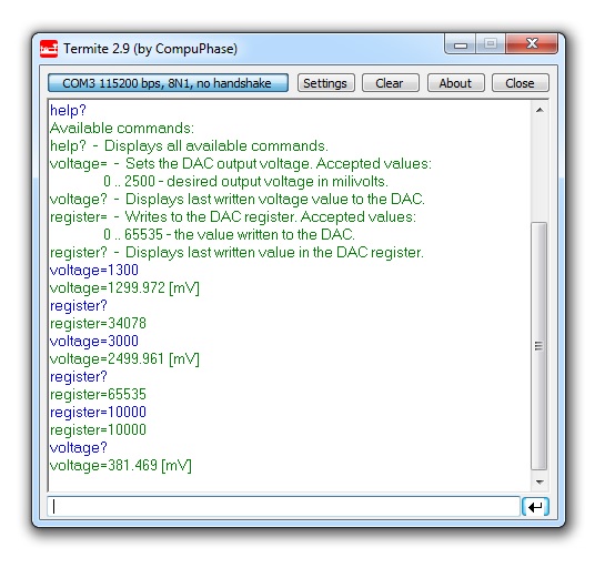
The following image shows a generic list of commands in a serial terminal connected to Xilinx KC705 FPGA's UART peripheral.

The hardware platform for each reference projects with FMC-SDP interposer and KC705 evaluation board is common. The next steps should be followed to recreate the software project of the reference design: