AD9789 Evaluation Board, DAC-FMC Interposer & Xilinx ML605 Reference Design
Introduction
The AD9789 is a flexible four channel QAM encoder, interpolator and upconverter combined with a high performance, 2.4GSPS, 14-bit, RF digital-to-analog converter (DAC). This reference design includes DDS generators that drives all channels of the device. The programming is done via the USB-SPI interface.
Supported Devices
Supported Carriers
Quick Start Guide
The bit file provided combines the FPGA bit file and the SDK elf files. It may be used for a quick check on the system. All you need is the hardware and a PC running a UART terminal, ADI DAC software and the programmer (IMPACT).
Required Hardware
Required Software
Bit file
Running Demo (SDK) Program
To begin make the following connections (see image below):
Connect the AD9789-EBZ board to the FMC Interposer board.
Connect the interposer board to the FMC-LPC connector of ML605 board.
Connect power to ML605 and the AD9789-EBZ boards.
Connect two
USB cables from the PC to the
JTAG and
UART USB connectors on ML605.
Connect a
USB cable to the AD9789-EBZ board.
Connect an external clock source to AD9789-EBZ board's S1 (HF_DACCLK) SMA connector.
Connect a spectrum analyzer to AD9789-EBZ board's S5 (AOUT_DAC-) SMA connector.
Setup the clock source to be 2.4GHz/6dBm. After the hardware setup, turn the power on to the ML605 and the AD9789-EBZ boards.

The reference design primarily supports four modes of operation.
| Mode | Key-Select | Bus-Width | Data-Width | Data-Format | First Block Enabled | Description |
| 0x0 | 'a' | 32 | 8 | Real | QAM mapper | Channelizer Mode. |
| 0x1 | 'b' | 32 | 8 | Complex | SRRC filter | Channelizer Mode. |
| 0x2 | 'c' | 32 | 16 | Complex | Interpolation Filter | Channelizer Mode. |
| 0x3 | 'd' | 32 | 16 | Complex | N/A | QDUC Mode. |
The reference design is NOT fully verified across all the modes. The delay/latency parameters may have to be adjusted depending on various features selected.
QAM Mapper Mode
SRRC Filter Mode
Interpolation Filter Mode
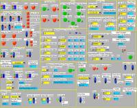
Start ADI- AD9789 SPI program (see screenshot below)-
Click on “Run Continously” button.
Interface Control: Set DCO_INV to OFF position (change it to ON if the spectrum has unwanted spurs).
Interface Control: Set I/F_MODE to Channelizer mode.
Interface Control: Set CHANPRI to ON position (enabled).
Data Control: Set Coding to Binary position.
Data Control: Set Data Width to 16-Bit mode.
Data Control: Set I/O-Data Path to Complex.
Data Control: Make sure BusWidth is set to 32.
Data Control: Set Latency to 1.
Channel Select: Enable all channnels.
Bypass: Enable QAM Mapper, SRRC filter and filter 4 bypass.
Summing Junction Scalar Input Scalar: Set 2.6 Multiplier Scale to 16. Note that this value must be set so that the saturation counter is always read as 0x0. You may clear the saturation register by clicking on the knob right next to it.
NCO Frequency Tuming Words: Make sure the central frequency is 834MHz on all channels.
Interpolating BPF Center Frequency: Set it to 834MHz click twice on the button to the right for the changes to take effect.
Reference/Sample/Sync Clock Control: Make sure DCODIV is set to 0x1.
Reference/Sample/Sync Clock Control: Set DSCPHZ to 0x0, click twice on PARAMNEW to take effect.
Reference/Sample/Sync Clock Control: Set SNCPHZ to 0x3, click twice on PARAMNEW to take effect.

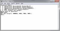
If programming was successful, you should be seeing messages appear on the terminal as shown in figure below.

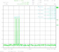
Select 'c' for the interpolation filter mode. The spectrum should appear as shown below. The DDS is set to 500KHz to 2000KHz.

QDUC Mode
Start ADI- AD9789 SPI program (see screenshot below)-
Click on “Run Continously” button.
Interface Control: Set DCO_INV to OFF position (change it to ON if the spectrum has unwanted spurs).
Interface Control: Set I/F_MODE to QDUC mode.
Interface Control: Set CHANPRI to ON position (enabled).
Data Control: Set Coding to Binary position.
Data Control: Set Data Width to 16-Bit mode.
Data Control: Set I/O-Data Path to Complex.
Data Control: Make sure BusWidth is set to 32.
Data Control: Set Latency to 1.
Channel Select: Enable channel 0, disable all the other channnels.
Bypass: Enable QAM Mapper, SRRC filter and all other filters bypass.
Summing Junction Scalar Input Scalar: Set 2.6 Multiplier Scale to 45. Note that this value must be set so that the saturation counter is always read as 0x0. You may clear the saturation register by clicking on the knob right next to it.
NCO Frequency Tuming Words: Make sure the central frequency is 834MHz on channel 0.
Interpolating BPF Center Frequency: Set it to 834MHz click twice on the button to the right for the changes to take effect.
Reference/Sample/Sync Clock Control: Make sure DCODIV is set to 0x1.
Reference/Sample/Sync Clock Control: Set DSCPHZ to 0x0, click twice on PARAMNEW to take effect.
Reference/Sample/Sync Clock Control: Set SNCPHZ to 0x3, click twice on PARAMNEW to take effect.

If programming was successful, you should be seeing messages appear on the terminal as shown in figure below.

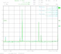
Select 'd' for the qduc mode. The spectrum should appear as shown below. The DDS is set to 3MHz.

Using the reference design
Functional description
The reference design consists of a DDS module and a lvds interface. The DDS module consists of a Xilinx DDS core and DDR based DDS. It is possible to change the output data delay with respect to the DCO clock, as well as the FS to data delay. See the regmap file and the SDK c file.
Registers
Refer to the regmap.txt file inside the pcore.
Downloads
Tar file contents
The tar file contains, in most cases, the following files and/or directories. To rebuild the reference design simply double click the XMP file and run the tool. To build SDK, select a workspace and use the C file to build the elf file. Please refer to Xilinx EDK documentation for details.
| license.txt | ADI license & copyright information. |
| system.mhs | MHS file. |
| system.xmp | XMP file (use this file to build the reference design). |
| data/ | UCF file and/or DDR MIG project files. |
| docs/ | Documentation files (Please note that this wiki page is the documentation for the reference design). |
| sw/ | Software (Xilinx SDK) & bit file(s). |
| cf_lib/edk/pcores | The pcores directory. |
