


This version (18 Jan 2024 13:26) was approved by Alin-Tudor Sferle.The Previously approved version (18 Jan 2024 13:25) is available.
AXI_PWM_GEN
The axi_pwm_gen core is used to generate a maximum of 16 configurable signals (Pulse-Width Modulations). The pulses are generated according to the state of a counter; there is one counter for each pulse.
Features
- Up to 16 configurable signals(period, width, offset)
- External synchronization
- External clock
The offset feature will synchronize counters 0, 1, 2, 3, 4, 5, 6, 7, 8, 9, 10, 11, 12, 13, 14, 15 to an offset counter.
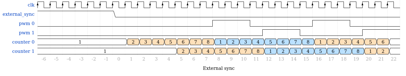
The axi_pwm_gen core can be synchronized by an external signal. The offset counter will wait for a HIGH → LOW transition of the synchronization pulse.
If another synchronization is needed, the external_sync signal should be set HIGH and the load_config should be toggled (by register write). This will cause the counters to wait for another external_sync HIGH → LOW transition.
To disable a PWM, write 0 to its period register.
Block Diagram

Configuration Parameters
| Name | Description | Default Value |
|---|---|---|
ID | Core ID should be unique for each IP in the system | 0 |
ASYNC_CLK_EN | Use external clock, asynchronous to s_axi_aclk | 1 |
N_PWMS | Number of pulses/pwms | 1 |
PWM_EXT_SYNC | PWM offset counter uses external sync | 0 |
EXT_ASYNC_SYNC | The external sync for pulse 0 is asynchronous | 0 |
PULSE_0_WIDTH | Pulse 0 width (number of clk cycles) | 7 |
PULSE_1_WIDTH | Pulse 1 width (number of clk cycles) | 7 |
PULSE_2_WIDTH | Pulse 2 width (number of clk cycles) | 7 |
PULSE_3_WIDTH | Pulse 3 width (number of clk cycles) | 7 |
PULSE_0_PERIOD | Pulse 0 period (number of clk cycles) | 10 |
PULSE_1_PERIOD | Pulse 1 period (number of clk cycles) | 10 |
PULSE_2_PERIOD | Pulse 2 period (number of clk cycles) | 10 |
PULSE_3_PERIOD | Pulse 3 period (number of clk cycles) | 10 |
PULSE_0_OFFSET | Pulse 1 offset (number of clk cycles) | 0 |
PULSE_1_OFFSET | Pulse 1 offset (number of clk cycles) | 0 |
PULSE_2_OFFSET | Pulse 2 offset (number of clk cycles) | 0 |
PULSE_3_OFFSET | Pulse 3 offset (number of clk cycles) | 0 |
PULSE_4_WIDTH | Pulse 4 width (number of clk cycles) | 7 |
PULSE_5_WIDTH | Pulse 5 width (number of clk cycles) | 7 |
PULSE_6_WIDTH | Pulse 6 width (number of clk cycles) | 7 |
PULSE_7_WIDTH | Pulse 7 width (number of clk cycles) | 7 |
PULSE_4_PERIOD | Pulse 4 period (number of clk cycles) | 10 |
PULSE_5_PERIOD | Pulse 5 period (number of clk cycles) | 10 |
PULSE_6_PERIOD | Pulse 6 period (number of clk cycles) | 10 |
PULSE_7_PERIOD | Pulse 7 period (number of clk cycles) | 10 |
PULSE_4_OFFSET | Pulse 4 offset (number of clk cycles) | 0 |
PULSE_5_OFFSET | Pulse 5 offset (number of clk cycles) | 0 |
PULSE_6_OFFSET | Pulse 6 offset (number of clk cycles) | 0 |
PULSE_7_OFFSET | Pulse 7 offset (number of clk cycles) | 0 |
PULSE_8_WIDTH | Pulse 8 width (number of clk cycles) | 7 |
PULSE_9_WIDTH | Pulse 9 width (number of clk cycles) | 7 |
PULSE_10_WIDTH | Pulse 10 width (number of clk cycles) | 7 |
PULSE_11_WIDTH | Pulse 11 width (number of clk cycles) | 7 |
PULSE_8_PERIOD | Pulse 8 period (number of clk cycles) | 10 |
PULSE_9_PERIOD | Pulse 9 period (number of clk cycles) | 10 |
PULSE_10_PERIOD | Pulse 10 period (number of clk cycles) | 10 |
PULSE_11_PERIOD | Pulse 11 period (number of clk cycles) | 10 |
PULSE_8_OFFSET | Pulse 8 offset (number of clk cycles) | 0 |
PULSE_9_OFFSET | Pulse 9 offset (number of clk cycles) | 0 |
PULSE_10_OFFSET | Pulse 10 offset (number of clk cycles) | 0 |
PULSE_11_OFFSET | Pulse 11 offset (number of clk cycles) | 0 |
PULSE_12_WIDTH | Pulse 12 width (number of clk cycles) | 7 |
PULSE_13_WIDTH | Pulse 13 width (number of clk cycles) | 7 |
PULSE_14_WIDTH | Pulse 14 width (number of clk cycles) | 7 |
PULSE_15_WIDTH | Pulse 15 width (number of clk cycles) | 7 |
PULSE_12_PERIOD | Pulse 12 period (number of clk cycles) | 10 |
PULSE_13_PERIOD | Pulse 13 period (number of clk cycles) | 10 |
PULSE_14_PERIOD | Pulse 14 period (number of clk cycles) | 10 |
PULSE_15_PERIOD | Pulse 15 period (number of clk cycles) | 10 |
PULSE_12_OFFSET | Pulse 12 offset (number of clk cycles) | 0 |
PULSE_13_OFFSET | Pulse 13 offset (number of clk cycles) | 0 |
PULSE_14_OFFSET | Pulse 14 offset (number of clk cycles) | 0 |
PULSE_15_OFFSET | Pulse 15 offset (number of clk cycles) | 0 |
Signal and Interface Pins
| Interface | Pin | Type | Description |
|---|---|---|---|
External clock | Clock signal | ||
ext_clk | input | Input clock | |
External sync | external sync signal | ||
external_sync, | input | Synchronize pulses to an external signal | |
PWM | pwm signals | ||
pwm_0 | output [1] | Output pwm 0 | |
pwm_1 | output [1] | Output pwm 1 | |
pwm_2 | output [1] | Output pwm 2 | |
pwm_3 | output [1] | Output pwm 3 | |
pwm_4 | output [1] | Output pwm 4 | |
pwm_5 | output [1] | Output pwm 5 | |
pwm_6 | output [1] | Output pwm 6 | |
pwm_7 | output [1] | Output pwm 7 | |
pwm_8 | output [1] | Output pwm 8 | |
pwm_9 | output [1] | Output pwm 9 | |
pwm_10 | output [1] | Output pwm 10 | |
pwm_11 | output [1] | Output pwm 11 | |
pwm_12 | output [1] | Output pwm 12 | |
pwm_13 | output [1] | Output pwm 13 | |
pwm_14 | output [1] | Output pwm 14 | |
pwm_15 | output [1] | Output pwm 15 | |
s_axi | AXI Memory Map interface | ||
Functionality
The axi_pwm_gen offers the possibility of four output signals (pwms). Pulse 0, 1, 2, 3, 4, 5, 6, 7, 8, 9, 10, 11, 12, 13, 14, 15 can have offsets in reference to the pwm counter.
The pulse generator is based on incrementing counters. In a pulse period, the first interval of the signal, until the level transition, the signal level is HIGH (pulse_width) and the second interval is LOW (pulse_period-pulse_width).
By default, all counters start at the same time. When a different phase (delay) is needed between the pulses, the offset value is calculated in number of clock cycles:
The below timing diagram, shows the external_sync functionality:
The timing diagram below, shows the load_config functionality:
All four pulses are active and all four pulses have the same period.

Register Map
PWM Generator (axi_pwm_gen)
resources/fpga/docs/axi_pwm_gen.txt · Last modified: 18 Jan 2024 13:26 by Alin-Tudor Sferle