


This version (08 Jan 2021 09:52) was approved by Ioana Chelaru.The Previously approved version (03 Jan 2021 22:04) is available.
Table of Contents
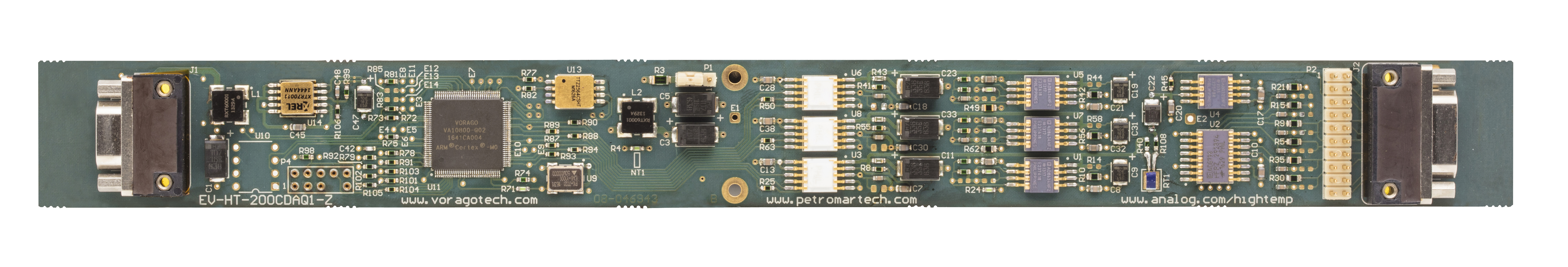
EV-HT-200CDAQ1 Hardware Design Notes
EV-HT-200CDAQ1 builds on the CN0365 analog front end reference design with the goal of providing a foundation for a high temperature, low power microcontroller-based data acquisition and control solution that meets the requirements for many downhole instrumentation and other high temperature applications. Based upon the AD7981 analog-to-digital SAR converter, this reference design demonstrates a full featured system with two high speed simultaneously sampled channels along with 8 additional multiplexed channels suitable for covering the acquisition requirements of a broad range of downhole tools (10 channels total). This analog front end is connected via SPI ports to the VA10800 ARM® Cortex®-M0 microcontroller from VORAGO Technologies, an Analog Devices Alliance Partner.

Once acquired, the data can be processed locally or transmitted via a UART or optional RS485 communications interface. Other supporting components on the board, including memory, clock, power and passives are all rated for high temperature operation by their respective suppliers and verified to operate reliably at 200°C or higher. The board layout, shown below, is approximately 11.4” long and 1.1” wide. This is a typical long-and-narrow form factor required for instruments that must be mounted in oil drilling and exploration equipment.
Powering the EV-HT-200CDAQ1
Power and communications interface signals are provided on the Micro-D 15 connector J1. The EV-HT-200CDAQ1-Z has flexible power options, but for best performance (comparable to the CN-0365 reference design) the board requires three power rails:

Note that these are nominal operating currents. Maximum current will be higher under different operating modes such as a flash programming cycle or high temperature conditions.
The system can be energized with other power configurations including 3.3 V only single supply operation but at compromised DC and AC performance or input signal range as headroom in the op-amps and multiplexer are reduced. These power modes are not characterized here but one can refer to the ADR225, AD8534, AD7981, and ADG798 data sheets for guidance.
There are two user configurable shunts that help facilitate alternate power configurations:

An input power filter attenuates interference from power lines, 3.3VIN and Vp, above 1700 Hz. It also attenuates conducted emissions from the digital components. A 33 nF capacitor, and series 100 Ω resistor on 3.3VIN and Vp terminate these lines so they don’t ring or oscillate in response to powerline emissions. Power input Vm uses a 10 Ω resistor in the line as input filtering element.
Analog Input Channel
The design of the data acquisition channel for the EV-HT-200CDAQ1 is covered extensively by theCN0365 application note. That design serves as the basis for the three ADC inputs on this platform, although some changes and optimizations were made, mostly in passive component selection, in order to address the form factor requirements of the board and extended reliable operation up to 200°C. The reference acquisition channel circuit is shown the schematic below. There are two “digital multiplexed” channels that each contain a complete data acquisition channel, similar to CN0365, that are capable of running at high sample rates. There is also an “analog multiplexed” channel that adds an ADG798 multiplexer in front of the inputs, optimized for lower throughput inputs. R1 and R3 provide a 1.25 V bias for the non-inverting input of U1, and prevent it from floating to the rail of the analog input if left open, or if the multiplexer is de-selected. R8 and R9 can be changed to increase the gain of U1. R4, R7, and C1 are the anti-aliasing filter, but they can be re-configured as an attenuator or alternate filter configuration. R5, R6, and C4 form the RC filter between the ADC driver and ADC input that limits the amount of out-of-band noise arriving at the ADC input and attenuates the kickback voltage from the switched capacitors in the ADC’s input.

All inputs provide a first order anti-aliasing filter consisting of a 249Ω and 2.7 nF RC filter with roll off at 237 kHz. This filter is set wide to accommodate high sample rate applications, but can be lowered with component changes for low sample rate applications using the provisions for attenuation and RC filtering at each input. Analog input signals should limit the applied voltage from ground to Vref (0V to 2.5V). The common-mode range of the AD8634 op-amps are specified at 300 mV above Vee, which will limit the input voltage range for the case of powering the board with +3.3VDC single supply. No input protection is provided internally on the board other than the 249Ω series resistance on the anti-aliasing filter. Current should be limited to no more than 5 mA if an over/under-voltage condition is expected. This includes situations where the main board is unpowered but input signals are still driven. External input protection diodes can be used, but should be applied carefully, because the leakage noise of the diodes at 200 °C may dominate the entire system.
All analog inputs are biased at ½ Vref by 100 kΩ voltage dividers, giving a 50 kΩ input resistance. This prevents un-connected inputs from floating away to the rail when not in use and allows AC-coupled inputs to be configured by adding only a series capacitor. Use a large value for this coupling capacitor, so its reactance does not amplify input-noise current. The 100 kΩ dividers were chosen over higher values to mitigate the effects of AD8634 input bias currents and ADG798 pin leakage as a DC input error source at high temperature. The input dividers form a resistor divider with the 249 Ω anti-aliasing filter which is an additional source of DC error. These effects can be compensated for by applying a scale correction factor in software.
This platform was designed to take advantage of several key features of the AD7981 ADC. This 16-bit, 600kSPS converter is capable of greater than 85dB typical SINAD and ±0.6 LSB typical INL with a 2.5V reference and no missing codes. Greater than 90dB SINAD can be achieved with a 5V reference, although that was not selected for this platform in order to maintain compatibility with lower voltage systems. Because the ADC core automatically powers down between conversion cycles, ADC power consumption automatically scales linearly with throughput. This allows power savings to be realized when using the converter at lower sampling rates.
One ADR225 voltage reference serves all three ADC. A 249Ω - 10ųF RC LPF network is provided, one for each channel, to reduce noise inherent in the ADR225 low power reference. Each channel is then buffered by an AD8634 going into the AD7981 ADC channel. The 33 µF solid-tantalum rservoir capacitors on the 2.5 V reference output buffers have been reduced in value from the original CN0365 design due to space constraints in the small form-factor PCB. Tantalum capacitors were used for the reservoir caps due to the extreme size of ceramic capacitors in large values.
Multiplexer Channel Measurements
General Input Channels
Six of the eight multiplexer channels are brought to the connector and available as general purpose inputs. Full sample rate is supported on this channel and in the most trivial configuration a single channel can be used as another high speed acquisition channel. In multiplexed operation mode, adequate settling time needs to be provisioned depending on measurement accuracy requirements. For the default input channel configuration a settling of 5 time constants corresponds to a 3.3 ųs minimum sampling period.
Vcc Measurement
Vcc is sampled on multiplexer channel 7, with respect to Vref and thus measurements that are ratio-metric to Vcc can be DC corrected.
RTD Measurement
A 1 kΩ RTD has been provided, and is connected to multiplexer channel S8. It is biased by two 1 kΩ resistors to Vref. The temperature-dependent voltage developed across the RTD is multiplexed into the ADC. Software converts the voltage to a temperature reading in degrees Celsius. RTD circuits has good repeatability, which is the most important factor for sensor calibration. However, accuracy will start deviating from true reading around 150°C. This is attributable to ADG798 mux leakage at these temperatures. At 200°C the RTD has sensitivity to leakage of 114nA / °C. The EV-HT-200CDAQ1-Z evaluation board design trades off RTD accuracy in order to eliminate the cost and space of an additional op-amp buffer in this design.
To mitigate the effects of mux leakage in a custom design several approaches can be taken:
- An andditional AD8634 op-amp buffer can be used between the RTD and the multiplexer to drive it with a low impedance source.
- A low leakage multiplexer can be used to prevent bias errors. ADG5298 is pin compatible with ADG798, and because of the dielectrically isolated process has dramatically lower leakage current, but requires higher supply voltage.
- An individual calibration can be performed to null the effect of mux leakage over temperature
- Lower value resistors and RTD can be used at the cost of higher power consumption
Headline
PCB Layout and Assembly
The EV-HT-200CDAQ1-Z was designed as a relatively low cost platform capable of serving as a serviceable evaluation and prototype platform and starting point for a high temperature system level design. As an evaluation platform has been tested at 200 °C operation 200 hours without failures or compromise to the assembly. While the board builds on the CN0365 reference design, certain design considerations are made to realize a practical multi-channel system that fits into a downhole form factor. All selected components are rated by the respective manufacturer for 200 °C operation unless otherwise indicated. Operating reliability and lifetime is ultimately driven by process and materials such as choice of solder, PCB substrate, conformal coatings, lead preparation, assembly process, etc. Each customer must apply their own standards and qualification parameters to consider a system qualified for their specific mission profile.
Capacitors
C0G/NP0 dielectric capacitors are used for low value filtering and decoupling. These dielectrics have a very flat coefficient over temperature and are generally more tolerant to board flexing stresses. Small footprint 0805 or less ceramics are used to minimize CTE mismatch between component and PCB.High temperature Tantalum capacitors are chosen for bulk energy storage with tradeoff considerations between footprint size and ESR.
Resistors
PATT series 0603 SMD footprints are the preferred choice but larger footprint sizes and alternate series were chosen primarily dictated by value and wide availability.
Inductors
Inductors were chosen for 200 °C operational rating and surface mount footprint.
Connectors
The board is connectorized with 200 °C rated Micro-D’s which are common in the downhole industry. To reduce signal crosstalk the shell of the connector can be grounded to the PCB in the assembly to the pad provided. For applications where the highest signal integrity and lowest crosstalk is required high temperature specialty connectors (or no connector) should be utilized that incorporate coaxial or shielded balanced inputs to minimize crosstalk.
Headers
A 250 °C rated Sullins IDC header is provided in the analog section to facilitate probing or the addition of an interface daughter board in bench test scenarios. A PCB mount female connector is available for the daughterboard assembly, or alternatively high temperature ribbon cable assemblies are also available.
Programming Sockets
The programming socket uses an array of 100 mil spaced brass/copper sockets, factory rated for 125 °C, but are suitable for survivability under 200 °C operation. Alternatively this PCB footprint will also accept a 5×2 IDC header in place of the socket array.
PCB
The PCB form factor was chosen for suitability in downhole applications, long and narrow, where circuit boards have to conform to the constraints of a borehole. Circuit board material chosen was a high temperature halogen free polyimide. 0.093” board thickness was specified for added rigidity and planarity over standard 0.062” thickness boards. A nickel-gold surface finish is used, where nickel provides a barrier that resists intermetallic growth, and gold provides a good surface for solder joint bonding. At these increased thicknesses a typical 4-layer stack-up will involve a ~13 mil copper layer separation with a large 60 mil internal core. At six layers, layer separation is typically 9.5-mil and 28-mil. For this reason a six layer design was utilized and allows a ground plane next to each signal layer for better noise performance.

Power and digital communication signals feed into one connector and analog signals come in on the opposing connector. This provides good isolation between digital and analog domains. The plane split is mid-board, with power filtering provided near the split. The digital control lines that do cross the split plane are minimized, and series terminations are provided to minimize coupling of digital noise. The digital and analog ground planes are bonded at a single point with a copper net tie to provide a low impedance return path to the driving sources. The multiplexer control signals run the length of the analog section but are routed to keep away from critical analog signal paths. In typical applications these multiplex control lines change synchronously with the acquisition measurement and crosstalk effects are minimized.
Solder
Sn95/Sb05 was chosen to provide a high enough melting point (>230 °C) over the 200 °C operational temperature and provide good workability and general assembly-house availability.
Board Mounting
The post mounts provided on this board are for convenience only, and are only useful for mounting in bench testing or lab situations. They are not suitable mounts for high shock and vibration environments. Mechanical testing was not included in the testing of this reference design. However, it is common in industry for high shock and vibration environments that the board can be prepared by first staking heavy components to the board with epoxy. Susceptible items like the IDC Headers can be encapsulated or removed from the assembly. Typical mounting would involve a rail mount system that secures the perimeter of the board with flexible shock mount gaskets. Alternatively the assembly can be fully encapsulated and potted inside mounting hardware that is then affixed to the chassis.
resources/eval/user-guides/high-temp/ev-ht-200cdaq1/hardware.txt · Last modified: 08 Jan 2021 09:52 by Ioana Chelaru