 This version (27 Feb 2019 03:50) is a draft.
This is an old revision of the document!
CN0414 is an Arduino compatible shield that provides a complete, fully isolated, highly flexible, quad channel analog input system suitable for programmable logic controllers (PLCs) and distributed control system (DCS) applications that require multiple voltage inputs and 4 mA to 20 mA current inputs. Additionally, the 4-20 mA inputs provide HART communication to remote field devices.
The circuit shown below uses AD4111, a low power, low noise, 24-bit, sigma-delta (Σ-Δ) analog-to-digital converter (ADC) that integrates an analog front end (AFE) for fully differential or single-ended rail-to-rail, bipolar, ±10 V voltage inputs, and 0 mA to 20 mA current inputs. The AD5700-1 is the industry’s lowest power and smallest footprint HART-compliant modem and is used in conjunction with the current input channels to form a HART-compatible, 4 mA to 20 mA receiver solution. The ADG704 multiplexer provides HART connectivity to the multiple current input channels. The ADuM5411 and ADuM3151 provide digital line and power isolation. The ADP2441 36 V, step-down, dc-to-dc regulator accepts an industrial standard 24 V supply, with wide tolerance on the input voltage and steps it down to 7.5V to be used by the system.
This user guide will discuss how to use the EVAL-EVAL-ADICUP3029 and evaluation software to configure and collect data from the EVAL-CN0414-ARDZ Evaluation Board (CN-0414 Board).
Terminal block P3 is the power supply input (input range:+9.5V to +36V DC). The EARTH terminal can be connected to an external earth connection, to the GND terminal or left floating if an external earth connection is not used.


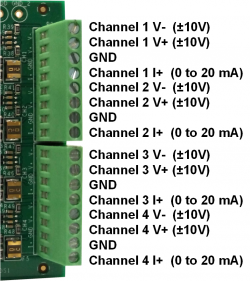
The analog input circuit is designed for group-isolated industrial analog inputs and can support voltage and current inputs in the following ranges:
| Range | Analog Input Terminals Description |
|---|---|
| * ±5 V |  |
| * ±10 V | |
| * 0 V to 5 V | |
| * 0 V to 10 V | |
| * 4 mA to 20 mA | |
| * 0 mA to 20 mA |
If only a single board is used, then connect jumpers P1 and P2 as shown in the table below.
If more than one board is stacked (up to 4), then each board must be set to a different ADC and HART select address. Connect jumpers P1 and P2 as shown in the table below, and ensure that the software is configured accordingly. (On a given board, set the ADC and HART address to the same position.)
If only a single board is being used, then ensure that JP1 Solder Jumper is shorting pins 2 & 3 as shown in the table below. If multiple boards are used, short pins 1 & 2.
Add some detail about what the LEDs mean when they are on or off? What is the standard operating condition they should be in?
EVAL-CN0414-ARDZ Design & Integration Files
End of Document