


This version is outdated by a newer approved version. This version (19 Dec 2013 12:42) is a draft.
Approvals: 0/1The Previously approved version (12 Dec 2013 17:09) is available.
This version (19 Dec 2013 12:42) is a draft.Approvals: 0/1The Previously approved version (12 Dec 2013 17:09) is available.
This is an old revision of the document!
CN-0233 Software User Guide
<fs medium>OVERVIEW</fs>
Industrial and instrumentation systems, as well as programmable logic controllers (PLCs) and distributed control systems (DCS), must often control outputs, which can be both current controlled (4 mA to 20 mA), and voltage controlled (up to ±10 V). Typically, such designs also need to be isolated from the local system controller to protect against ground loops and also to ensure robustness against external events. Traditional solutions use discrete ICs for both power and digital isolation. When multichannel isolation is needed, the cost and space of providing discrete solutions becomes a big disadvantage. Solutions based on opto-isolators typically have reasonable output regulation but require additional external components, thereby increasing board area. Power modules are often bulky and may provide poor output regulation. The circuit is based on the ADuM347x family of isolators (ADuM3470, ADuM3471, ADuM3472, ADuM3473, ADuM3474) and integrates digital isolation, as well as the PWM-controlled power regulation circuitry along with associated feedback isolation. External transformers are used to transfer power across the isolation barrier. The AD5422 16-bit DAC provides the current and voltage outputs.
<fs medium>GENERAL SETUP</fs>
- EVAL-CN0233-SDPZ Evaluation Board
- EVAL-SDP-CB1Z Evaluation Board
-
- (supplied with provided CD in kit)
- +6V DC power supply
- USB Type-A plug to USB Mini-B plug cable
- Power supply: +6 V, Agilent E3630A or equivalent
- Digital Multi Meter
<fs medium>MINIMUM PC/SYSTEM REQUIREMENTS</fs>
- One PC with the following
- Windows XP SP2, Windows Vista or Windows 7 Business/Enterprise/Ultimate editions
- Intel Pentium processor (x86 compatible), 1GHz or faster
- 512 MB RAM and 2 GB available hard disk space
- .NET 3.5 Framework
<fs medium>HOW TO INSTALL THE EVALUATION SOFTWARE</fs>
- Extract the file CN0233 Eval Software.zip and open the file setup.exe.
NOTE: It is recommended that you install the CN0233 Evaluation Software to the default directory path C:\Program Files\Analog Devices\CN0233\ and all National Instruments products to C:\Program Files\National Instruments\

- Click Next to view the installation review page
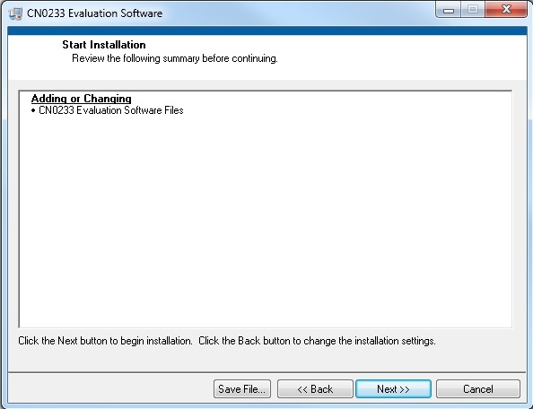
- Click Next to start the installation

- Upon completion of the installation of the CN0233 Evaluation Software, the installer for the ADI SDP Drivers will execute.
NOTE: It is recommended that you close all other applications before clicking “Next”. This will make it possible to update relevant system files without having to reboot your computer.
- Press “Next” to set the installation location for the SDP Drivers.
It is recommended that you install the drivers to the default directory path
C:\Program Files\Analog Devices\SDP\Drivers

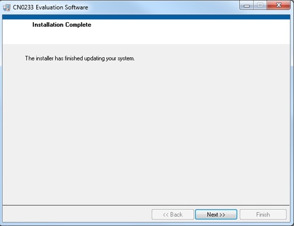
- Press “Next” to install the SDP Drivers and complete the installation of all software. Click “Finish” when done.


<fs medium>STEP BY STEP INSTRUCTION FOR CONNECTING THE HARDWARE</fs>

- Connect the 120-pin connector on the EVAL-CN0233-SDPZ circuit board to the connector marked “CON A” on the EVAL-SDP-CB1Z evaluation (SDP) board. Nylon hardware should be used to firmly secure the two boards, using the holes provided at the ends of the 120-pin connectors as depicted in the image below.
- Connect a voltmeter to Vout of EVAL-CN0233-SDPZ.
- Connect a current meter to Iout of EVAL-CN0233-SDPZ.
- To power on the EVAL-CN0233-SDPZ, connect the +6V DC power supply to P2, using a wallwart power supply, or to P3, using bench supply.
- Connect the USB cable, supplied along with the EVAL-SDP-CB1Z evaluation board, from the SDP board to the USB port on the PC.
—-
<fs medium>OPENING AND ENABLING THE EVALUATION SOFTWARE</fs>
- Launch the executable found at C:\Program Files\Analog Devices\CN0233 and press the “Connect” button.
- After pressing the “Connect” button, a prompt will appear informing the user that the SDP is now ready to acquire data and the rest of the buttons found in System Controls will be enabled.
- Press the “Run” button in order to start using the program.
<fs medium>STEP BY STEP INSTRUCTION USING THE EVALUATION SOFTWARE</fs>
Below are the list of available software controls grouped according to their location in the software GUI:
- System Controls
- Run – This button writes configuration found in the Advanced Configuration tab to the AD5422 control register and the data written at the Output Range, found in the Block Diagram tab, to the data register.
- Reset Register – This button reset the register of the of AD5422
- Main Tab – This tab contains displays for the Block Diagram, Advance Configuration and SDP Board Firmware Revision.
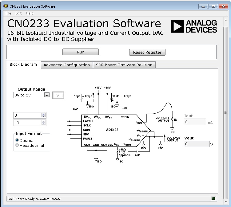
- Block Diagram – This page contains the AD5422 block diagram that generates the voltage or current output after configuring the output range, writing the desired data and clicking the Run button found in the system control.
- Output Range – This drop menu configure the output range of the AD5422 by selecting the desired output shown in the menu.
- Input Format – This set the input type, in hex or decimal input, to the data register of the AD5422.
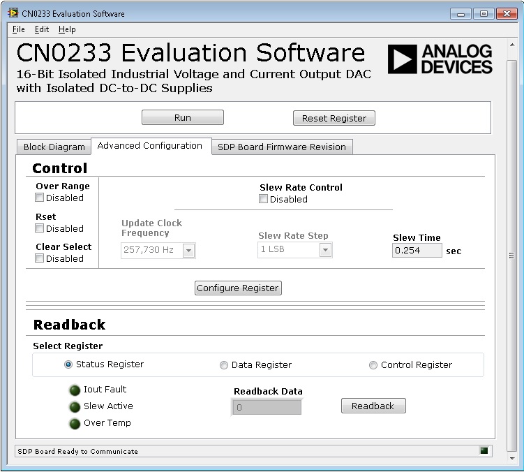
- Advance Configuration – This page contains the controls necessary to configure the control register of the AD5422.
- Control – This section of the page shows the control registers which can be configure according to the users application.
- Over Range – Setting this bit increases the voltage output range by 10%.
- Rset – Setting this bit selects the external current setting resistor.
- Clear Select – an active high clear that allows the voltage output to be cleared to either zero-scale code or midscale code.
- Slew Rate Control – enable control register needed to configure the slew rate of the analog output.
- Update Clock Frequency – defines the rate at which the digital slew is updated.
- Slew Rate Step – defines by how much the output value changes at each update.
- Slew Time – shows the time it takes for the output to slew over a given output range
- Configure Register – this configures the control resigter set in this control section of this page and the output range set in the Block Diagram page.
- Readback – This section of the page shows the available read only registers for AD5422.
- Readback Registers
- Status Register – read the status of the Iout Fault, Slew Active, Over Temp
- Iout Fault – This bit is set if a fault is detected on the IOUT pin.
- Slew Active – This bit is set while the output value is slewing (slew rate control enabled).
- Over Temp – This bit is set if the AD5412/AD5422 core temperature exceeds ~150°C.
- Data Register – This configures the part for read mode with the data register selected.
- Control Register – This configures the part for read mode with the control register selected.
- Readback Data – This message box display the data read from the selected read registers.
- Readback – This triggers the readback operation when clicked.
- SDP Board Firmware Revision – provides details on the firmware version of the Blackfin used by the SDP board.


resources/eval/user-guides/circuits-from-the-lab/cn0233.1387453320.txt.gz · Last modified: 19 Dec 2013 12:42 by erbe reyta