


This version (27 Sep 2022 15:49) was approved by Emrecan Gidik.
Table of Contents
DC2610A ACE Software User Guide
Description
Demonstration circuit 2610A features the LTC6953, an Ultralow Jitter, a 4.5GHz Clock Distributor with 11 Outputs, and JESD204B Support. By default, the DC2610A is powered by a single 3.3V supply. An option is provided to power to the DC2610A from dual supplies, allowing for the LTC6953’s output supply pins to connect to an LTC Silent Switcher® and the LTC6953 input supply pin to connect to a low noise LDO. All differential inputs and seven of the differential outputs are populated with 0.5” spaced SMA connectors. These outputs are AC-coupled with 50Ω transmission lines making them suitable to drive 50Ω impedance instruments. The remaining four differential outputs are terminated with 100Ω.
The LTC6953’s EZSync™ and SYSREF request functions are available via the LTC6953 SPI interface or the EZS_SRQ SMA/turret connectors. The DC2610A SMA placement was designed for ease of connection for all multi-part synchronization and SYSREF request modes.
A calibration path is provided to aid in accurate LTC6953 propagation delay measurements.
A DC2026 USB serial controller board is used for SPI communication with the LTC6953, controlled by the ACE™ software and LTC6953 Plugin.

Figure 1: DC2610A Board View and Connections
Getting Started
The DC2610A is easy to set up to evaluate the performance of the LTC6953. Follow the procedure below. The ACE Software and the DC2026 are required to control the DC2610A through a personal computer (PC)
DC2026 Linduino Board Configuration
Refer to Figure 2. Set the JP3 jumper to the 3.3V (preferred) or 5V position. Connect the DC2026 to one of your computer’s USB ports with the included USB cable. The DC2026 has the ability to run Linduino code, refer to Design Center.

Figure 2: DC2026 Board View and Connector Locations
ACE and Plugin Installation
You can install the LTC6953 plug-in from the ACE start-up page. You can install ACE from ACE Software Page
- On the ACE start-up page locate and click the Plug-in Manager on the sidebar.
- Select Available Packages from the panel second sidebar
- Search for Board.LTC6952 and install plug-in

Figure 3: ACE Plugin Search Screen
Evalutaion Board Setup
- Connect J30, J32, and J33 to the appropriate power supplies and apply power (see Figure 1 and the Typical DC2610A Requirements and Characteristics table).
- Connect the DC2026 to the DC2610A with the provided ribbon cable
- Run the ACE application. Double click the LTC6953 icon that appears on the Attached Hardware tab when the DC2026 board is connected and attached to the board. If the icon does not appear, consider re-installing the LTC6953 plug-in or try refreshing the Attached hardware icon.
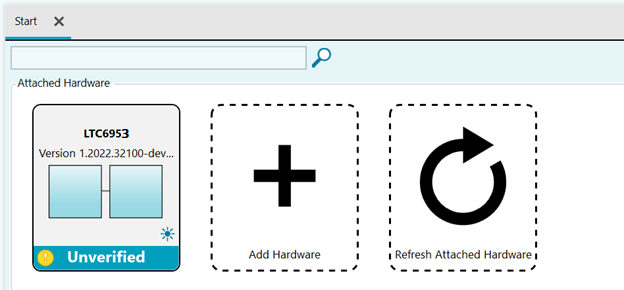
Figure 4: Attached Hardware Tab
- Connection is automatically established with DC2026. You can navigate to board and chip view.
- Double Click the LTC6953 Board Icon and the tab shown in Figure 5 appears.
- Double click the LTC6953 icon that appears on the LTC6953 Board tab to open main control window shown in Figure 6.

Figure 5: LTC6953 Board View on ACE Software
General Software Features
In chip view, one can find various control features of LTC6953. One can read and control all registers mentioned in the LTC6953 datasheet. Register Hb00 can easily be read by clicking the “Check Status Register” button. Small LED icons will be lit if the register bit value is high. Stat Pin output mask register value can be set visually to reflect which information will be carried to Stat Pin Output. The clock distribution circuit consists of eleven paths. Each path can be controlled individually. SRQEN bit, MODE, Power-down modes, divider value, digital delay, and analog delay of each channel can be modified from the chip view. EZsync mode and SYSREF features can be controlled from the chip view. EZSync Mode, SRQ Mode, and SysRef Pulse count can be adjusted. The main controls are available in the high-level register map shown in Figure 7. To modify registers, perform the following steps:
- Modify the registers as desired.
- Click Apply Changes to load the modified settings to the device. This action loads the updated registers only.
By clicking Proceed to Memory Map button or Memory Map Side-By-Side button, register values can be seen.

Chip View of LTC6953 on ACE Software
CML Outputs, OUT[10:0]
The DC2610A has 11 CML outputs. Seven of these outputs are AC-coupled and brought out to SMAs (OUT10, OUT9, OUT8, OUT5, OUT4, OUT1, and OUT0). To drive 50Ω impedance instruments connect OUTx+ to the instrument and OUTx– to a 50Ω termination, or vice versa. The remaining four outputs (OUT7, OUT6, OUT3, and OUT2) are terminated with a 100Ω resistor onboard. To connect these outputs to a 50Ω instrument, remove the 100Ω termination, and install the appropriate SMAs and AC blocking capacitors. Refer to the LTC6953 data sheet for differential termination options.
Typical DC2610A Requirements and Characteristics
| Parameter | Direction | Physical Location | Details |
|---|---|---|---|
| 3V3 Power Supply | Input | J30 and J31 BNC Banana Jack | If R4 Populated, Default Option, Single Supply: 3.3V Low-noise and spur-free supply, 1.5A; If R4 Depopulated, Dual Supply Option, allows for experiments with more efficient power supply evaluation (LTC Silent Switcher). See 3.3V Power Supply #2 (VIN33) |
| 3V3 Power Supply #2 (VIN33) | Input | E23 Turret | If R4 Depopulated, Dual Supply Option, 3.3V Lownoise and spur-free supply, 150mA |
| GND | Output | J33 Banana Jack | Pair with J30 and J32 |
| OUT9+; OUT9- | Output | J3 and J4 SMA* | CML, AC-Coupled, 800mVpk Differential |
| OUT8+; OUT8- | Output | J5 and J6 SMA* | CML, AC-Coupled, 800mVpk Differential |
| OUT5+; OUT5- | Output | J19 and J20 SMA* | CML, AC-Coupled, 800mVpk Differential |
| OUT4+; OUT4- | Output | J17 and J18 SMA* | CML, AC-Coupled, 800mVpk Differential |
| OUT1+; OUT1- | Output | J11 and J12 SMA* | CML, AC-Coupled, 800mVpk Differential |
| OUT0+; OUT0- | Output | J9 and J10 SMA* | CML, AC-Coupled, 800mVpk Differential |
| OUT10+; OUT10- | Output | J1 and J2 SMA* | CML, AC-Coupled, 800mVpk Differential |
| OUT7+; OUT7- | Output (Not Connected) | J7 and J8 SMA* | Onboard Differential 100Ω termination |
| OUT6+; OUT6- | Output (Not Connected) | J21 and J22 SMA* | Onboard Differential 100Ω termination |
| OUT3+; OUT3- | Output (Not Connected) | J15 and J16 SMA* | Onboard Differential 100Ω termination |
| OUT2+; OUT2- | Output (Not Connected) | J13 and J14 SMA* | Onboard Differential 100Ω termination |
| IN+ | Input (Not Connected) | J29 SMA Connector | Default: Not Connected |
| IN- | Input | J28 SMA Connector | Default: Preferred Single Ended Input |
| EZS_SRQ+ | Input | J27 SMA Connector, E20 Turret | Default: Preferred Single Ended Input |
| EZS_SRQ- | Input | J26 SMA Connector, E19 Turret | Default: Shorted to Ground |
| IDS | Input | Test Point | 3.3V(Default): Device Active, set by pull-up resistor GND: Shut Down Device |
| STAT | Output | STATUS Turret | Red LED D1 illuminates when STAT pin in high state |
*Any unused RF output must be powered down or terminated with 50Ω, or poor spurious performance may result. 1Not Populated
Troubleshooting
If the red LED(D1) does not illuminate
- Ensure the LTC6953 input signal is at the LTC6953 IN– pin.
- In ACE Chip View, click “Check Register Status”. STAT Output Pin should match STAT Pin Mask And Output.
Verify DC2610A and LTC6953 Plugin Communication:
To verify communication with the DC2610A, Go to the start page or system view page and click the button shown below.

Figure 7: Attached Hardware Tab on ACE
LEDs on the Serial Interface Boards don’t light up, then perform the following steps:
- Ensure the DC2026 is connected to the PC
- Disconnect and Reconnect DC2026 to PC
- Ensure DC2026 is connected to DC2610A
- Close ACE and Restart
- Verify the DC2026 has the DC590B Emulator Sketch loaded by contacting the factory or following these steps.
- Run QuickEval (Linduino connected to PC)
If QuickEval does not find a DC590B, reload the DC590 Linduino sketch To use the LTSketchbook refer to the Linduino Design Center for instructions on how to start using Linduino
resources/eval/ltc6953-ace-software-guide.txt · Last modified: 24 Aug 2022 13:22 by Emrecan Gidik