


This version (03 Jan 2021 21:10) was approved by Robin Getz.The Previously approved version (09 Mar 2015 18:07) is available.
Table of Contents
AD9577 Evaluation Board User Guide
Evaluation Board Features
- Simple power connection using 6V wall adapter and on-board LDO voltage regulators
- 2 ac-coupled differential output SMA connectors terminated for LVPECL
- 1 ac-coupled differential output SMA connector terminated for LVDS
- 1 ac-coupled differential output SMA unterminated connector
- 1 ac-coupled single ended reference output connector
- 1 dc-biased input reference SMA connector
- USB connection to PC
- Microsoft Windows-based evaluation software with simple graphical user interface
- Pin/I2C programmable
- Status LEDs
Equipment Needed
- Reference oscillator or signal generator
- Other evaluation board to be clocked or test equipment
- Oscilloscope, spectrum analyzer, phase noise analyzer
- SMA cables (50 Ω)
- 6 V wall supply (provided)
- USB cable (provided)
Online Resources
GENERAL DESCRIPTION
The AD9577 evaluation board is a compact, easy-to-use platform for evaluating all features of the AD9577. The AD9577 provides a multioutput clock generator function, along with two on-chip phase-locked loop cores, PLL1 and PLL2, optimized for network clocking applications. The PLLs have I2C programmable output frequency/format and an array of physical control pins that can be turned on and off on the evaluation board.
The AD9577s four differential outputs can be driven by an on board 25MHz crystal or through an SMA connector. The output differential transmission line pairs use 50Ω single ended characteristic impedance and are connected to standard edge launch SMA connectors. The AD9577 evaluation board uses RoHS-compliant FR-4 material. For convenience, detailed information from the AD9577 data sheet has been included here. Use this user guide in conjunction with the AD9577 data sheet and software documentation available at www.analog.com.

Figure 1. AD9577-EVALZ
EVALUATION BOARD HARDWARE
The following instructions are for setting up the physical connections to the AD9577-EVALZ evaluation board. The user must install the evaluation software prior to connecting the evaluation board for the first time.
Power and PC Connections
- Install AD9577 evaluation software, uninstall prior versions of the software before installation updates. Administrative privileges are required for installation.
- Connect the 6V wall power supply to the main power connector labeled P12.
- Connect the USB cables to the evaluation board and the computer. The red LED labeled CR1 on the AD9577 evaluation board should illuminate and LEDs CR2 and CR3 should blink.
- If the Found New Hardware Wizard window automatically appears when the evaluation board is connected, select Install the software automatically and click Next.
- The Found New Hardware Wizard window may appear twice, and a system restart may be required.
Refer to the Evaluation Board Software section for details on running the AD9577 evaluation board software.
Signal Connections
XO Input
- The on AD9577 evaluation board comes with a 25MHz crystal oscillator that can be used as a reference input. To use the on board XO as a reference, the REFSEL pin should be driven to VDD (Jumper P9) and the REFCLK input should be grounded (Jumper P11).
REFCLK Input
- The AD9577 can use a single-ended reference through the SMA connector J1 (REFCLK). The REFCLK input is selected when the REFSEL pin is driven low (Jumper P9). The board’s default state is REFSEL driven high. Jumper P11 must also be removed.
Outputs
- The CMOS REFOUT output (J2) of the AD9577 will be a copy of the applied REFCLK.
- Connect an oscilloscope, spectrum analyzer, or other lab equipment to any of the J2 to J10 SMA clock OUT connectors on the board.
- OUT0 and OUT1 are terminated as ac-coupled LVPECL outputs 150Ω to ground. OUT2 is terminated as an ac-coupled LVDS output.
- OUT3 and REFOUT are only ac-coupled. The board can easily be converted to dc-coupled traces by replacing the capacitor with a zero Ohm surface-mount resistor.
Default Evaluation Board Setup
- REFSEL pin (P9 ) set to VDD, selecting the XO for the REFCLK input.
- MARGIN pin (P8) is set to VSS, turning margining off.
- SSCG pin is set to VSS, turning spread spectrum modulation off.
- MAX_BW pin is set low, selecting the normal bandwidth of 50kHz for PLL2.
- 25MHz crystal oscillator connected to the XO inputs is populated.
- REFCLK input (J1) is ac-coupled and terminated with a 50Ω resistor to ground which is then dc biased to VDD/2.
- OUT0 and OUT1 are terminated as ac-coupled LVPECL outputs 150Ω to ground.
- OUT1, OUT3, and REFOUT are only ac-coupled.
EVALUATION BOARD SOFTWARE
Use the following instructions to set up the AD9577 evaluation board software.
Software Installation
Do not connect the evaluation board until the software installation is complete.
- The latest evaluation software and documentation can be downloaded from http://www.analog.com/en/clock-and-timing/clock-generation-and-distribution/ad9577/products/EVAL-AD9577/eb.html. Download the AD9577 Evaluation Software.zip.
- Once downloaded, double-click setup.exe inside of the Volume folder. (Note that the website may have a newer version.) Follow the installation instructions.
Running the Software
Power up and connect the evaluation board to the PC. See the Evaluation Board Hardware section for details on the various connectors on the evaluation board. At start up, the graphical user interface (GUI) displays the dialog shown in Figure 2. The software allows the user to work online with an evaluation board or to work offline without an evaluation board. When working offline, the user can adjust all of the AD9577 settings and create configuration files for later use when an evaluation board is available.

Figure 2. Dialog Shown at Start Up
Online Mode
When Run In Online Mode is selected, the main panel is displayed as in Figure 3. The title bar displays “Online Mode”. Most of the interface is disabled until I2C communication is verified by clicking the Check Connection button in the upper-left corner.
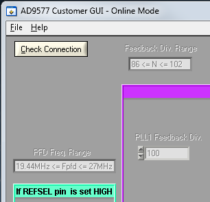
Figure 3. Check Connection Button in Main Window
After clicking Check Connection and I2C communication is working, the GUI panel is fully enabled and loaded with the default values for the part. The software is now ready to change the AD9577 settings and features such as output frequencies, output formats, and spread spectrum settings. The fully enabled Main Window is shown in Figure 4 in the Evaluation Software Components section of this user guide.
Offline Mode
When Run In Offline Mode is selected, the panel loads with default values and all controls enabled except the Acquire button. The title bar displays “Offline Mode”. The same controls are available as in online mode; however, they do not actually perform any I2C writes. The Check Connection button is also not present. Offline mode can be used to generate a setup file, which can be later used in Online Mode. See the Evaluation Software Components section for a description of the evaluation software features.
Setup Files
To create a setup file:
- Start the software in online mode and verify I2C communication or start the software in offline mode.
- Adjust the AD9577 settings for the desired configuration.
- Select the File/Save Setup As menu item. Select an output filename and the file will be written.
- If the AD9577 power is cycled, the Reset DUT button is clicked, or the program is re-launched from offline to online mode, the saved settings can be recalled by using the File/Open Setup menu item. The settings in the file will be written to the AD9577.
EVALUATION SOFTWARE COMPONENTS
Main Window
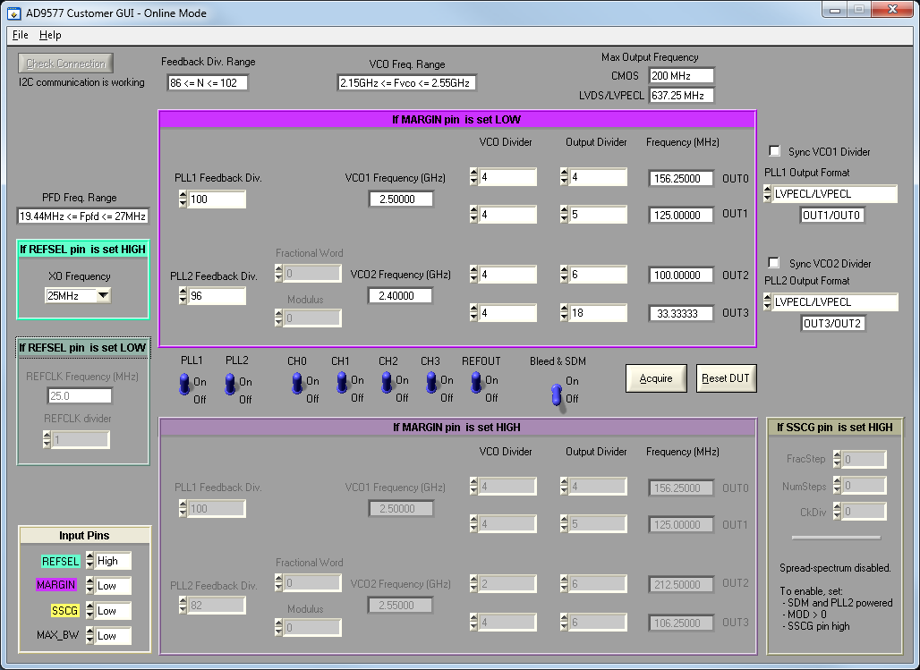
Figure 4. Evaluation Software Main Window
Active and Inactive Controls
Many controls are active only under certain conditions. Input pin states and power switches determine which controls are active. Active controls are displayed with a white background, while inactive controls have a grey background as shown in Figure 5.


Figure 5. Active Control vs. Inactive Control
Unlike many Windows programs, inactive controls can still be edited and still cause the registers to be changed in the AD9577 (in Online mode). This is to support applications where the part configuration may be switched dynamically (such as when MARGIN or REFSEL are controlled by a microcontroller).
Invalid Value Indication
Certain combinations of values can cause the AD9577 operating parameters to exceed the valid ranges as specified in the datasheet. In some of these cases, the GUI will highlight invalid values in red.
The following conditions are checked within the software:
- The PFD frequency must be between 19.44MHz and 27MHz
- Feedback dividers (N) must be chosen so that the VCO frequency is valid
- Feedback dividers should not equal each other for the same value of MARGIN (injection locking)
- VCO frequencies must be between 2.15GHz and 2.55GHz
- CMOS output frequency must not be greater than 200MHz
- LVDS/LVPECL output frequency must not be greater than 637.5MHz
- REFCLK divider must be set to 1 when using the crystal (when REFSEL is high)
- SSCG must not cause FRAC/MOD to roll over more than 4 times, i.e.,
- SSCG downspread only supported from -0.5% to 0.0%.
Figure 6 shows the result when several invalid values have been selected. The invalid values and the constraints that have been violated are highlighted in red. Note that there may be additional requirements specified on the datasheet that are not validated by the user interface.

Figure 6. Main Window with Invalid Settings
Input Pins Control
The input pin controls are located in the lower-left corner of the GUI (Figure 7). The software controls only affect the appearance of the GUI. To change the state of these pins, you must adjust the jumpers on the evaluation board. Setting the input pin controls to match the evaluation board setup allows the proper controls to be displayed as active. Table 1 outlines each input pin and the corresponding section that it appears in within this user guide.

Figure 7. Input Pin Configuration
| Input Pin Name | Section Within User Guide |
|---|---|
| REFSEL | Input Frequency Section |
| MARGIN | PLL and Output Divider Section |
| SSCG | Spread Spectrum Section |
| MAXBW | Please Refer to the AD9577 Datasheet |
Table 1. Input Pin Name and Corresponding User Guide Section
Input Frequency Section
The input frequency section of the Main Window is used to identify which input reference (XO or REFCLK) is being used and the frequency of that reference. By default, REFSEL is set to High and the input frequency section will look like the left side of Figure 8. The XO Frequency drop-down is used to select which frequency of crystal oscillator is connected to the AD9577. When REFSEL control is set to Low, the panel will look like the right hand side of Figure 8.


Figure 8. Input Frequency Controls
The external REFCLK frequency being used should be typed into the text box under REFCLK Frequency (MHz). The software expects that a reference clock between 19.44MHz and 27MHz is externally given to the AD9577 when REFCLK divider=1 is used. If any other value outside of this range is entered into REFCLK frequency, the software will turn controls red to signify that the REFCLK frequency is too high. It is possible to apply a reference frequency between 38.88MHz and 54MHz if REFCLK divider is set to 2.
When the REFCLK divider=1 the REFCLK is applied directly to both PLLs. When REFCLK divider=2 the REFCLK is divided by two before being applied to both PLLs. It is important to remove the jumper that shorts the REFCLK input to ground (P11) when the REFCLK is in use. It is also important to know that the CMOS REFCLK output of the AD9577 will be a copy of the applied REFCLK and not the divided down REFCLK.
PLL and Output Divider Section
The PLL and Output Divider Section of the Main Window shown in Figure 9 is used to set the various divider values in both of the AD9577 PLLs. This section also calculates output frequency based on the reference frequency and divider values entered by the user. Selecting Margin equal to High or Low in the Input Pins Control causes the selected Margin setting to illuminate. By default, MARGIN is low and only the top central section (labeled “If MARGIN pin is set LOW”) is active. The other section can be edited, but it will not have any effect on the operation of the AD9577 until the MARGIN pin jumper (P8) is adjusted.
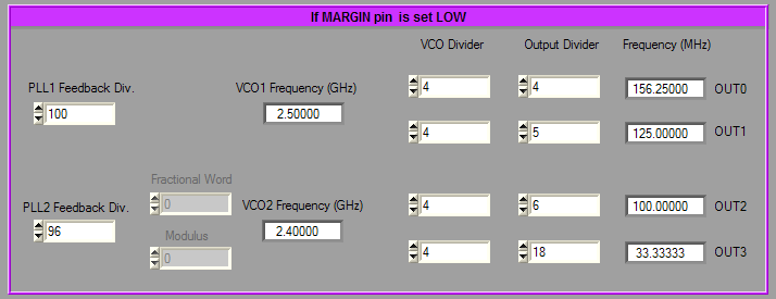

Figure 9. PLL and Output Divider Controls when MARGIN is Low
The top half of each group contains the PLL1 controls. PLL1 is an integer-N PLL and the VCO1 frequency is the product of the input frequency and the feedback divider. PLL2 powers up as an integer-N PLL but it is possible to use it as a Frac-N PLL. In Integer-N mode, VCO2 frequency is calculated the same as VCO1 frequency. When PLL2 is run in fractional-N PLL mode, the effective feedback divider is adjusted by the fractional word and the modulus registers as described in the equation below.
To set PLL2 to fractional-N mode, the BLEED & SDM switch shown in Figure 10 must be turned on. When it is turned off, the FRAC and MOD boxes are grayed out.

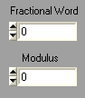
Figure 10. Bleed & SDM Switch with Corresponding FRAC/MOD control
It is important to note that the PLL1 and PLL2 feedback dividers should not be set equal to each other. This could cause reduced performance due to injection locking between the two VCOs. The output frequencies are calculated by dividing the VCO frequency by the product of the corresponding VCO Divides and Output Divider.
Margining
The Margin pin can be switched from low to high by adjusting the MARGIN Jumper on the evaluation board (P8). It is a good idea if you are using PLL2 as a Frac-N PLL when MARGIN is high that PLL2 is also being used as a Frac-N PLL when MARGIN is low. Figure 11 shows how the PLL and Output Divider Section changes when MARGIN is switched to High within the software.
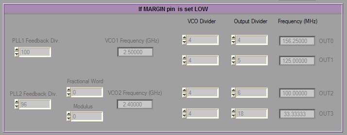
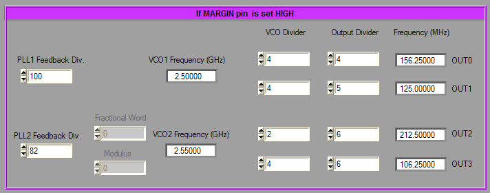
Figure 11. PLL and Output Divider Controls when MARGIN is High
Output Format and SYNC Section
The Output Format and SYNC section allows the user to adjust the PLL1 or PLL2 output formats and SYNC settings. Figure 9 shows the Output Format and SYNC section of the Main Window. To change which output format is used, select the desired format from the dropdown menu. Table 2 shows the possible output formats supported by the AD9577. The format is specified as OUT1/OUT0 or OUT3/OUT2.

Figure 12. Output Format and SYNC Controls
| Output Formats |
|---|
| LVPECL/LVPECL |
| LVDS/LVDS |
| 2xCMOS/LVPECL |
| 2xCMOS/2xCMOS |
| 2xCMOS/LVDS |
| LVPECL/LVDS |
| LVPECL/2xCMOS |
| *2xCMOS/2xCMOS |
Table 2. Supported Output Formats
*all four CMOS ouputs per PLL are in phase
Changing output format only adjusts the output drivers of the AD9577. The LVPECL termination resistors need to be removed for LVDS or CMOS operation. It is important to note that it is not possible to have different output formats for the different states of the MARGIN pin.
When the SYNC check boxes are selected, the display will appear as shown in Figure 13. The VCO Divider boxes for OUT1 and OUT3 become shaded because when SYNC is checked, OUT0/OUT1 share a VCO divider and OUT2/OUT3 share a VCO divider. It is important to note that when SYNC is checked, the sync occurs for both states of the MARGIN PIN.
 Figure 13. Display When Both SYNC Options are Checked
Power ON and OFF Switches Section
This section of the GUI panel allows the user to turn sections of the AD9577 off and on. There are on and off switches for the following: PLL1, PLL2, CH0 Output, CH1 Output, CH2 Output, CH3 Output, and the REFOUT output. When each switch is turned off, the GUI display also updates to indicate which controls will not have any effect. For example, if PLL1 and CH3 are both turned off, the display will look like Figure 14, indicating that only OUT2 will have a signal.

Figure 14. Effect of On/Off Switches on the Main Window
Spread Spectrum Section
The Spread Spectrum Section can be illuminated in the Main Window by changing SSCG to High in the Input Pins Control Section. The right side of Figure 15 shows the illuminated section.
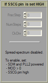
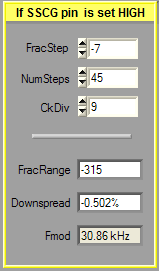
Figure 15. Spread Spectrum Register Display
Spread spectrum mode is physically enabled on PLL2 by adjusting the SSCG Jumper (P7) on the evaluation board such that the SSCG pin is high. PLL2 must be in Fractional-N mode for spread spectrum operation to function. The output frequency is modulated with a triangular profile and the peak power is reduced. The tri-wave modulation is implemented by controlling the divide ratio of the feedback divider. This is achieved by ramping the fractional word to the SDM.
The key parameters that define the frequency modulation profile are:
- FracRange: The maximum change in the modulated FRAC value from the initial FRAC value.
- Downspread: The maximum percent reduction in output frequency for OUT2 and OUT3.
- Fmod: The frequency of the modulation waveform
The following equations determine the value of the above parameters:
The following are programmable registers that affect the previous equations:
- FracStep: The value of the fractional word decrement while traversing the tri-wave. Only negative values are supported.
- NumSteps: The number of fractional word steps in half the tri-wave period.
- CkDiv: The refclk frequency is divided by this integer value to determine the update rate of the tri-wave generator, i.e. the step update rate.
The default values for FracStep, NumStep, and CkDiv are all 0 and must be modified before spread-spectrum operation will function.
Acquire and Reset Buttons
The Acquire button in the Main Window forces the AD9577 to perform a new acquisition. The Reset button resets the AD9577 back to its default power up state. After a reset, the feedback dividers, VCO dividers, output dividers, output format, output sync, SSCG registers and on/off switches are all returned to their default settings. Figure 16 shows the Acquire and Reset buttons.


Figure 16. Acquire and Reset Buttons
EVALUATION SOFTWARE MENU ITEMS
File Menu
The File menu has the following options:
- Reset To Defaults
- Open Setup
- Save Setup As
- Reset to Last Setup File
- Export JSON
- Exit
Reset To Defaults
Selecting Reset to Default resets the AD9577 to its default power-up state. This is the same as the Reset DUT button in the Main Window.
Open Setup
Selecting Open Setup reads a setup (.stp) file and applies the saved register settings to the AD9577. A setup file is a text file that contains the AD9577 register settings.
Save Setup As
Selecting Save Setup writes a setup (.stp) file containing all of the register settings currently loaded in the AD9577.
Reset to Last Setup File
This selection is only valid after performing one of the previous two actions. This sets the registers of the AD9577 back to the last opened or saved configuration.
Export JSON
Selecting Export JSON creates a file used for automatic programming in certain applications. This is not typically used.
Exit
Exits the evaluation software. No checking is performed to ensure that the existing setup is saved.
Help Menu
The Help Menu only contains the About section which shows the a short summary of the software being used.
resources/eval/ad9577-user-guide.txt · Last modified: 03 Jan 2021 21:04 by Robin Getz