


This version (28 Oct 2025 17:37) was approved by Petre Minciunescu.The Previously approved version (05 Oct 2021 12:49) is available.
Table of Contents
AD9544 Evaluation Board User Guide
Evaluation Board Features
- Simple power connection using 6V wall adapter and on-board LDO voltage regulators.
- 10 ac-coupled single-ended (differential signal recombined via a balun) output SMA connectors, with user-configurable output termination for HCSL, CML, or LVDS-compatible (default).
- 4 configurable reference inputs, selectable between a single ended to differential reference input SMA connector.
- 1 ac-coupled single-ended input SMA connector for system clock.
- On-board EEPROM, power on ready configurability.
- Status LEDs.
- USB connection to PC.
- Microsoft Windows-based evaluation software with simple graphical user interface via an ACE plug-in module
Equipment Needed
- Reference oscillator or signal generator for reference input
- Other evaluation board to be clocked or test equipment
- Oscilloscope, spectrum analyzer, phase noise analyzer
- 50 Ω SMA cables
- 6 V wall supply (provided)
- USB cable (provided)
Online Resources
Required Software
- AD9544 ACE Plug-in Module: board.ad9544.1.1.8.zip
- Please only use ACE Software version 1.10.2671.1118. Do not update it to newer versions as they are not tested with the AD9544 plug-in module
- Install ACE first. Unzip the plug-in. Double click on it to have it installed
Documents Needed
GENERAL DESCRIPTION
The AD9544 evaluation board is a compact, easy-to-use platform for evaluating all features of the AD9544 dual digital PLL and 1 PPS synchronizer. The AD9544 provides high-precision, multi-output clock generator functions, along with two on-chip jitter cleaning digital PLL cores. PLL0 and PLL1 are optimized for high performance synchronous clocking applications such as IEEE 1588 Version 2, Synchronous Ethernet, OTN, and next generation wireless baseband protocols. The PLLs are fully configurable via serial port control as well as configurable via an external EEPROM for power on ready configurations.
The AD9544 can output up to 5 differential clock signals, plus two single-ended clocks driven by a mix of two high performance digital PLLs, plue two high-precision NCOs (numerically controlled oscillators). 12 total outputs and 4 reference inputs are accessible on the evaluation board.
The output differential transmission line pairs use 50Ω single ended characteristic impedance and are connected to standard edge launch SMA connectors. The AD9544/PCBZ has a fully configurable power supply to allow the user to evaluate the AD9544 while being powered directly by a step down switching regulator or external LDOs. The AD9544 evaluation board uses RoHS-compliant FR-4 material. For convenience, detailed information from the AD9544 data sheet has been included here. Use this user guide in conjunction with the datasheet that has been provided by ADI.

Figure 1. AD9544 Evaluation Board
EVALUATION BOARD HARDWARE
The following instructions are for setting up the physical connections to the AD9544/PCBZ evaluation board. The user must install the evaluation software prior to connecting the evaluation board for the first time.
Power Connections
The AD9544/PCBZ is set up by default to power the AD9544 and remaining circuitry using the provided 6V wall power supply.
The 6V supply powers the following:
- An Analog Devices ADP2384A Switching Regulator configured to output 1.8 or 3.3V.
- A dedicated Analog Devices 3.3V ADP7104 Low Noise LDO for cases in which the user wishes to evaluate the AD9544 with an ultra-quiet power supply.
- A dedicated Analog Devices 3.3V ADM7171 Low Noise LDO for an on-board 3.3V OCXO. (1.0A, max)
- A dedicated Analog Devices 5V ADM7171 Low Noise LDO for an on-board 5V OCXO.(1.0A, max)
By default, the 3.3V ADP2384A switcher output supply supplies a 1.8V Analog Devices ADP7104 Low Noise LDO to power the AD9544. The ADP2384A Switching Regulator can alternately be configured to output 1.8V and directly power the AD9544 to evaluate the AD9544 when powered with a switching power supply.
- AD9544 Powered by ADP2384A Step-down Switching Regulator cascaded with ADP7104 LDO (Default):
- Remove P802 (sets switcher output voltage to 3.3 V)
- Remove P712/P728 (disconnects switcher output from VDD_DUT_EXT & VDD_DUT_IO_EXT)
- Install P704/P725/P727 to pins 1/2 (connects VDD_DUT & VDD_DUT_IO/VDD_MPIN to LDO output)
- Install P701/P721/P729 to pins 1/2 (enables LDOs that are being bypassed)
- AD9544 Powered by 1.8V ADP2384A Step-down Switching Regulator Directly:
- Install P802 (sets switcher output voltage to 1.8 V)
- Install P712/P728 (connects switcher output to VDD_DUT_EXT & VDD_DUT_IO_EXT)
- Change P704/P725/P727 to pins 2/3 (connects VDD_DUT & VDD_DUT_IO/VDD_MPIN to VDD_DUT_EXT & VDD_DUT_IO_EXT)
- Change P701/P721/P729 to pins 2/3 (disables LDOs that are being bypassed)
PC Connections
- Install all required software, uninstall prior versions of the software before installation updates.
Administrative privileges are required for installation. - Connect the 6V wall power supply to the main power connector labeled P700.
- Connect the USB cables to the evaluation board and the computer. The red LED labeled DS301 by the USB connector should illuminate and the LED labeled 'USB_STA' should blink.
- If the Found New Hardware Wizard window automatically appears when the evaluation board is connected, select Install the software automatically and click Next.
- The Found New Hardware Wizard window may appear twice, and a system restart may be required.
Refer to the Evaluation Board Software section for details on running the AD9544 evaluation board software.
Reference Inputs
The AD9544 evaluation board has four reference inputs sources. By default, REF A/AA (Connectors J300 and J301, respectively) have a transformer so that the user can use a signal generator and use REFA in differential mode.
In contrast, REF B/BB (Connectors J302 and J303, respectively) are configured for single-ended CMOS inputs by default. Each reference input logic type is configurable via the evaluation software. * REF B is intended for a DC-coupled, 1.8V/1.2V CMOS input and is terminated with only a 50Ω resistor to ground. * REF BB is intended for a either a DC-coupled, 5V CMOS input, and the on board voltage divider will decrease the input amplitude to 1.8V, or a 3.3V CMOS input which will be reduced to a 1.2V CMOS signal.
System Clock Inputs
By default, the AD9544 system clock input is configured to the on-board 49.152 or 50 MHz crystal. For applications that require either a TCXO or OCXO, The user use can select. Refer to Table 3 for the jumper settings to configure the serial port.
Table 3. System Clock Input Configuration
| SYSCLK Input | Jumper P402 | Jumper P403 |
|---|---|---|
| Crystal | Center and Right Pins | Center and Right Pins |
| TCXO | Center and Left Pins | Center and Left Pins |
| OCXO | Center and Top Pins | Center and Bottom Pins |
| J400 SMA Connector | Center and Bottom Pins | Center and Top Pins |
Serial Port Configuration Pins
The AD9544 serial port configuration is determined by the logic state of Multi-function pins M4, M5, and M6 upon exit from a reset state. M4 selects which protocol (SPI versus I²C), and M5 and M6 determine the I²C address. Jumper Block P605 allows the user to enable pull-up/down resistors to control the state of Pins M4, M5, and M6 on the AD9544. Refer to Table 4 for the jumper settings to configure the serial port.
Table 4. Serial Port configuration
| Serial Protocol | Slave Address | Jumper P605, Top/Middle/Bottom Row | Jumper P504 | Jumper P511 |
|---|---|---|---|---|
| SPI | N/A | Jumpers removed | SCLK | SDIO |
| SPI | N/A | 7-8 / 4-5 / 1-2 | SCLK | SDIO |
| I²C | 0x48 | 7-8 / 4-5 / 2-3 | SCL | SDA |
| I²C | 0x49 | 7-8 / 5-6 / 2-3 | SCL | SDA |
| I²C | 0x4A | 8-9 / 4-5 / 2-3 | SCL | SDA |
| I²C | 0x4B | 8-9 / 5-6 / 2-3 | SCL | SDA |
EEPROM Loading at Power-up
The AD9544 uses pin strapping of the M3 pin at reset or power-up to enable/disable EEPROM loading. To load the external EEPROM, place a jumper across the center and right pin of the top row of Jumper Block P604. This corresponds to Pins 10 and 11 in Jumper Block P604.
EVALUATION BOARD SOFTWARE
The AD9544 evaluation software allows the user to control the full functionality of the AD9544 through 3-wire SPI communication with the evaluation board. The AD9544 evaluation software is implemented as a component plug-in in ADI’s Analysis | Control | Evaluation (ACE) Software desktop software. ACE allows the evaluation of control of multiple evaluation systems from across ADI’s product portfolio and is designed to educate the user in the functional operation of the component. The ACE wiki page contains system requirement and prerequisite information as well as links to the most recent installer and user guide. The ACE user guide contains detailed information concerning all current aspects of the ACE environment. Much of that information will not be described in this document, but some main ACE operational points relevant to component level functionality will be described. It is highly recommended to review the ACE user guide to discover the myriad capabilities and offerings the ACE environment provides to the user.
Software Installation
Use the following instructions to set up the AD9544 evaluation board software.
Do not connect the evaluation board until the software installation is complete.
- Download and install ACE Software Version 1.10.2671.1118 Analysis | Control | Evaluation (ACE)
- Follow the section 2.1, installation guide, of the ACE User Guide to completion.
- Launch the ACE application prior to installing ACE Plug-ins. This creates the directories used by the ACE Plug-in installers.
- Download and install the latest AD9544 ACE Plug-ins: board.ad9544.1.1.8.zip
(Note that there are a total of four plug-ins that must be installed. Please unzip it first)
General Operation
Power up and connect the evaluation board to the PC. Open the ACE software. After opening ACE, the user will be presented with the Start View shown in Figure 2. The Explore Local Plug-ins section shows all plug-ins that are locally installed and allows the user to operate the plug-in without the presence of the associated evaluation platform. The Attached Hardware section shows all ADI evaluation platforms which are found to be connected to the PC. The appearance of an Unknown Hardware plug-in means that the plug-in for a detected ADI evaluation platform is not locally installed. Double click on any of the shown plug-ins will open the associated plug-in and navigate to its default view, which is the board view for the AD9544. Note: opening a plug-in from the Explore Local Plug-ins section will not automatically establish a connection with the associated evaluation platform even if the hardware is connected. Only opening a plug-in from the Attached hardware section will automatically establish this connection.
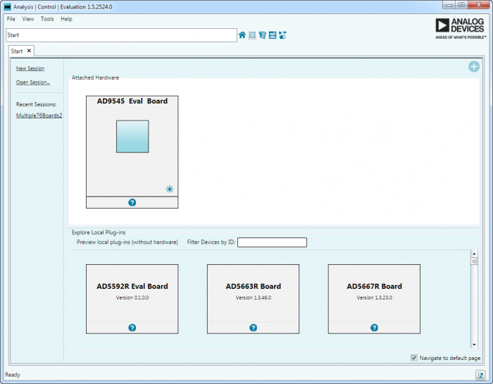 Figure 2. ACE Start Screen (AD9545 Shown)
Board View
The AD9544 board view can be seen in Figure 3. As the AD9544 evaluation platform is for a single component, the board view has only two main portions, as shown in Figure 3:
- View toolbar
- AD9544 primaray component link

Figure 3. AD9542/43/44/45 ACE Plug-in Board View (AD9545 Shown)
The board view toolbar provided three board level functions and a detailed description may be found in section 3.6.3 of the ACE user guide. The AD9544 primary component link allows the user to navigate to the AD9544 chip view, shown in Figure 4, by double clicking this link. The chip view is the primary conduit through which the user can interface with the AD9544.
Chip View
 Figure 4. AD9542/43/44/45 ACE Plug-in Chip View (AD9545 Shown)
The chip view is the primary interface used to configure the AD9544. It consists primarily of an interactive block diagram which shows the configuration of the device, calculates the frequency translation, implements frequency based error checking, and allows the user to intuitively configure the AD9544 parameters. It should be noted that in order to synchronize the register content of the software with that of the AD9544, the user must press the ‘Read All’ button in the chip view toolbar in the upper left hand portion of the window.
Configuration Wizard
The configuration wizard simplifies configuring the AD9544 by providing the most commonly needed configuration parameters in a simple user interface. Entered parameters are plugged into a powerful algorithm that calculates the optimal settings ensuring the best possible performance from the AD9544.
The wizard is made up in multiple collapsible1) steps. Each step contains parameters, which are used by the wizard algorithm to calculate an optimized configuration.
Invalid parameters are outlined in red with an error indicator2) in the upper left of the parameter, mouse-over the error indicator for an error description. Example see Figure 5 - OUT0B Expression
Once the desired parameters have been entered and all errors3) have been cleared, the Apply button may be clicked to apply the configuration to the chip.
 Figure 5. Configuration Wizard
Numeric Expressions
Some parameters can be entered using expressions.
Expression Format
An expression in it simplest form has three parts, a number followed by the SI prefix and Units. The units are not significant.
[Number][SI Prefix][Unit]
or
[Number][Space][SI Prefix][Unit]
For example.
| Expression | Evaluated Value |
|---|---|
| 1.25MHz | 1.25 MHz |
| 1+0.25 MHz | 1.25 MHz |
Supported SI Prefixes
Prefix  Value   Name
  Y     10e24   yotta
  Z     10e21   zetta
  E     10e18   exa
  P     10e15   peta
  T     10e12   tera
  G     10e9    giga
  M     10e6    mega
  k     10e3    kilo
  m     10e−3   milli
  u     10e−6   micro
  n     10e−9   nano
  p     10e−12  pico
  f     10e−15  femto
  a     10e−18  atto
  z     10e−21  zepto
  y     10e−24  yocto
A space between the number and SI prefix applies the SI prefix to all numbers in the expression.
| Expression | Evaluated Value |
|---|---|
| 1+0.25 MHz | 1250000 Hz |
| 1+0.25MHz | 250001 Hz |
The following table has some example expressions and evaluated values.
| Expression | Evaluated Value | Note |
|---|---|---|
| 1+1 Mhz | 2 MHz | SI prefix is applied to all numbers. |
| 2+1MHz | 1.000002 MHz | |
| 1+1/2 MHz | 1.5 MHz | |
| (1+1)/2 MHz | 1 MHz | Order of operations example. |
| 15/2*10 MHz | 75 MHz | |
| 15M/2M*10M Hz | 75 MHz |
Block Interaction
A detailed explanation of the interaction with the block diagram is explained in the ACE User Guide sections 3.7.1 through 3.7.3. However, it should be noted that the AD9544 chip view heavily leverages the use of configuration menus for blocks with multiple associated bit fields. Clicking on such a block will pop up a menu as pictured in Figure 6.
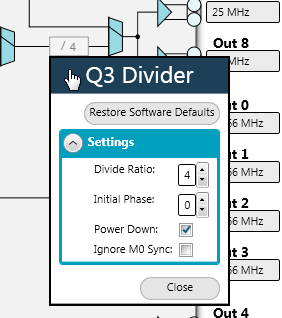
Figure 6. Divider Q3 Configuration Menu
Clicking and dragging the title bar of the menu will allow the user to relocate the menu at one’s convenience. In order to close the menu, the user may close the ‘close’ button or simply click away from the menu.
Frequency Translation Calculations
The frequency translation of the AD9544 is calculated from reference input frequency to output clock frequency based on the state of the intermediate blocks in between. Not every block in the block diagram impacts the frequency translation, but those that do contain a tool tip displaying the input and output frequencies associated with said block as illustrated in Figure 7.
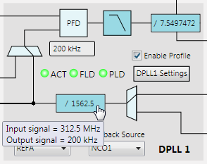
Figure 7. Frequency Display Tool Tip.
Changing the configuration of a block that affects the frequency translation will produce an automatic calculation and error checking to inform the user of the impact the change has had on the operation of the AD9543. Any errors resulting from the error checking functionality will display visually as well as the Events Tool View. This view gives the user additional detail regarding the nature of the error and is explained in detail in the ACE User Guide, section 3.9.3.
Memory Map View
The AD9544 ACE plug-in as contains a detailed view of the entire register map in either register or bit field based format, known as the Memory Map shown in Figure 8. This view may be accessed by clicking the ‘Proceed to Memory Map’ button in the lower right hand corner of the chip view.

Figure 8. AD9542/43/44/45 ACE Plug-in Memory Map View. (AD9545 shown)
The memory map view is explained in detail in the ACE User Guide section 3.8, but one of the more useful features in the functional group filter shown in the left portion of Figure 8. The AD9544 bit fields have been grouped by relevant functionality and the functional group filter allows the user to quickly and easily switch between viewing only bit fields or registers contained within these macro level functional groups.
Sessions
The ACE application has the ability to save and recall a given configuration of the software including all currently open plug-ins.
These ‘states’ are referred to as ‘sessions’. The File selection in the application toolbar contains options to create, open, save, or close sessions, as shown in Figure 9.

Figure 9. ACE File Menu.
The left hand section of the Start View also exposes the ability to create and open sessions as well as maintaining a list of recent sessions that may be directly opened.
Known Issues
- Please only use ACE Software Version 1.10.2671.1118 that can be downloaded here: ACE Version 1.10.2671.1118 Installer
EVALUATION BOARD QUICK START USING A SESSION FILE
This quick start section covers the loading of a session file as provided by ADI.
- Ensure the ACE evaluation software and AD9544 ACE Plug-ins are installed and running.
- Click File > Open Session…, and select the appropriate .cso file.
- In the AD9544 Chip View Toolbar, click the Apply Changes button.
- Apply a 0 dBm signal to the J301 SMA connector (REF0P) at a frequency corresponding to your AD9543 setup. This may also be applied prior to the session load.
- The APLL VCO calibration is a part of the register programming and will occur automatically after the session file is loaded.
resources/eval/ad9544-user-guide.txt · Last modified: 10 Aug 2022 18:32 by Petre Minciunescu