


This version (08 Jul 2021 22:28) was approved by Petre Minciunescu.The Previously approved version (09 Jan 2021 00:22) is available.
Table of Contents
AD9528 Evaluation Board User Guide
Features
- Simple power connection using 6 V wall adapter and on-board voltage regulators.
- Multiple power configurations to evaluate performance with buck regulators and/or LDO regulators.
- Prepopulated VCXO with universal pad.
- Universal pad allows for various VCXO package sizes to be used and evaluated.
- 2 reference input SMA connectors
- 2 ac-coupled single-ended SMA output connectors(2 differential paths)
- 12 ac-coupled differential SMA output connectors (6 differential paths)
- SYSREF SMA connectors for:
- External SYSREF
- External SYSREF Request
- USB connection to PC
- Microsoft Windows-based evaluation software with simple graphical user interface (supports 64-bit versions of Windows)
Equipment Needed
- Reference oscillator or signal generator
- Other evaluation board to be clocked or test equipment
- Converters, DDS, transceivers
- Oscilloscope, spectrum analyzer, phase noise analyzer
- SMA cables (50 Ω)
- 6 V wall supply (provided)
- USB cable (provided)
Online Resources
Required Software
Documents Needed
General Description
This user guide describes specific functionality of the AD9528 evaluation board hardware and evaluation board software. General software features including software installation instructions are covered in the Clock Generation and Distribution Evaluation Software User Guide. The AD9528 evaluation board is a compact, easy-to-use platform for evaluating all features of the AD9528 JESD204B Clock Generator. The AD9528 is a dual loop jitter cleaner and clock generator with internal SYSREF generator compliant with JEDEC JESD204B for multi-device synchronization. The AD9528 can output up to 14 clock signals, with any output configurable to PLL1direct out, PLL2, or SYSREF. 8 total outputs, 2 reference inputs, and a SYSREF input are accessible on the evaluation board. The AD9528/PCBZ has a fully configurable power supply to allow the user to evaluate the AD9528 while being powered directly by buck regulators or external LDOs. Use this user guide in conjunction with the AD9528 data sheet and software documentation available at www.analog.com.

Figure 1. AD9528/PCBZ
Evaluation Board Hardware
The following instructions are for setting up the physical connections to the AD9528/PCBZ. The user must install the evaluation software prior to connecting the evaluation board to their PC.
Power Connections
The AD9528/PCBZ is setup by default to power the AD9528 and remaining circuitry using the provided 6V wall power supply connected to drive an Analog Devices ADP5052 5-channel integrated power solution which is configured to output 3.3V and 5V from two internal buck regulators. The evaluation board can be configured to power the AD9528 with one of three on board power configurations as shown in Table 1.
Table 1. Power Supply Configuration Jumper Settings
| Configuration Name | Settings | ||
|---|---|---|---|
| Jumper P9 | Jumper P10 | Jumper P11 | |
| 3.3V LDO powered by 5V buck converter output (Default) | Set to position 1 (Enable) | Set to position 1 (LDO) | Set to position 1 (Filter) |
| 3.3V Buck Converter Output Through Passive Filter Network | Set to position 3 (Disable) | Set to position 3 (Switcher) | Set to position 1 (Filter) |
| 3.3V Buck Converter Output Direct | Set to position 3 (Disable) | Set to position 1 (LDO) | Set to position 3 (Switcher) |
PC Connections
The following instructions assume that the power supply is correctly configured to one of the three configurations discussed in the Power Connections section.
- Connect the wall power supply to the main power connector labeled P500.
- The red LED labeled 3V3_USB (DS4) will illuminate.
- The green LED labeled RESETB (DS3) will illuminate.
- Connect the USB cable to the evaluation board and computer.
- The red LED labeled CR300 on the AD9528 evaluation board will illuminate.
- The red LED labeled USB_STATUS (CR2) will blink once the evaluation board has successfully communicated with the PC.
Refer to the Evaluation Board Software section for details on running the AD9528 evaluation board software.
Signal Connections
Inputs
The AD9528/PCBZ has preinstalled connections for REFA, REFB, VCXO_IN, SYSREF_IN, and SYSREF_REQ. REFA and REFB are accessible via SMA connectors J27 and J4. A 0dBm sinusoidal input may be connected to these inputs to provide a reference signal to PLL1 of the AD9528. The AD9528 can create an internally generated SYSREF signal or can provide a buffered external SYSREF by applying signals to SYSREF_IN via SMA connectors J6 and J7. A third SYSREF option allows an external trigger to initiate SYSREF pulse from the internal SYSREF generator. The SYSREF_REQ pin is accessible by 3 paths on the evaluation board:
- Using an External Signal on SMA Connector J30
- Jumper P6 set to position 3 (EXTERNAL REQUEST)
- Using Push Button S1
- Jumper P6 removed.
- Using the Evaluation Software GUI to Access the Pin Through the USB Controller
- Jumper P6 set to position 1 (USB CONTROLLER REQUEST)
A low phase noise VCXO with single ended 3.3V CMOS output is populated by default. The AD9528/PCBZ allows the user to use an external VCXO evaluation daughter board by utilizing J14 which is connected to the AD9528 VCXO_VT pin and J101 which can be shorted to the AD9528 VCXO_IN_P pin. The path connected to J101 can also be used to provide a reference to PLL with an external 3.3V CMOS source. A third path allows the AD9528 to be configured as an asynchronous generator by using a small 3.3V CMOS XO on Y1. The following steps detail how to configure the AD9528/PCBZ for the three different VCXO_IN input options:
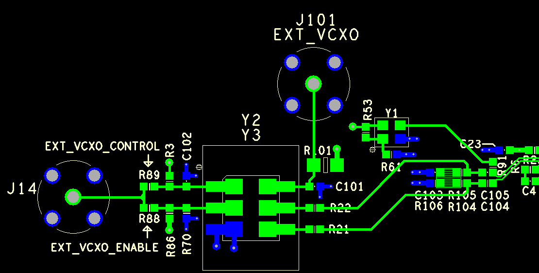
Figure 2. VCXO_IN Input Options
- Using an External 3.3V CMOS VCXO Daughter Board
- 1st Option: Connect J101 to VCXO_IN_N
- Remove VCXO (Y2), R101, C101
- Short VCXO pads 6 and 4
- 2nd Option: Connect J101 to VCXO_IN_P
- Remove VCXO (Y2), R101, C101, and R105
- Populate R22 with a 0 Ω resistor
- Populate R104 with a 100 nF capacitor
- Replace C105 with a 0 Ω resistor
- Short VCXO pads 5 and 6
- In both options, connect J14 to VCXO_VT
- Populate C102 = 470 nF and R89 = 0 Ω
- Using an External 3.3V CMOS Source
- 1st Option: Connect J101 to VCXO_IN_N
- Remove VCXO (Y2), R101, and C101
- Short VCXO pads 6 and 4
- 2nd Option: Connect J101 to VCXO_IN_P
- Remove VCXO (Y2), R101, C101, and R105
- Populate R22 with a 0 Ω resistor
- Populate R104 with a 100 nF capacitor
- Replace C105 with a 0 Ω resistor
- Short VCXO pads 6 and 5
- Using an On-Board 3.3V CMOS XO
- Remove C105, and R21
- Populate R91 = 0 Ω
- Populate R104 with a 100nF capacitor
- Populate Y1
- Populate R53 = 3.9 kΩ
Outputs
Connect an oscilloscope, spectrum analyzer, or other lab equipment to any of the horizontal OUTx inputs on the edge of the board. OUT0, OUT1, OUT11, and OUT12 are differentially terminated with 100Ω and ac coupled to SMA connectors J10-J13 and J34-J37. OUT4, OUT5, OUT8, and OUT9 are differentially terminated with 100Ω and combined to one output via a balun to SMA connectors J18, J20, J26 and J29. Baluns T8 and T13 can be removed and shorted so that both the positive and negative outputs from OUT4 and OUT9 can be connected to SMA connectors.
Evaluation Board Software
The AD9528 evaluation software allows the user to control the full functionality of the AD9528 through SPI communication on the evaluation board and a fully interactive software GUI. Please see the Clock Generation and Distribution Evaluation Software User Guide for general information on installing and running the software including software features that are redundant across multiple Clock and Distribution products.
Evaluation Board Software Components
The AD9528 evaluation software allows the user to control the full functionality of the AD9528 through SPI communication on the evaluation board. This section will detail device specific features of the AD9528 evaluation software. Generic software functionality is covered in the Clock Generation and Distribution Evaluation Software User Guide.
Main Window

Figure 3. AD9528 Evaluation Software Main Window
AD9528 Evaluation Board Quick Start
The quick start section covers only simple PLL operation to lock both AD9528 PLLs and output two high speed sample clocks and two SYSREF signals. See the AD9528 data sheet and Evaluation Software Components section for a detailed explanation of the various AD9528 features.
Table 2 describes a summary of one possible operating mode of the AD9528 which is setup used for this quick start guide.
Table 2. Quick Start Summary
| Parameter | Value |
|---|---|
| Input Frequency | 122.88MHz on REFA |
| Output Frequency | 122.88MHz on OUT0 and 245.75MHz on OUT10 |
| SYSREF Frequency | 960kHz on OUT1 and OUT11 |
| SYSREF Type | Internally generated 4 Pulse N-Shot |
| PLL1 Reference Divider | 4 |
| PLL1 Phase Detector Frequency | 30.72MHz |
| PLL1 External VCXO Frequency | 122.88MHz |
| PLL1 Feedback Divider (N Divider) | 4 |
| PLL2 Phase Detector Frequency | 122.88MHz |
| PLL2 VCO Frequency | 3686.4MHz |
| PLL2 Feedback Divider (N Divider) | 10 |
| PLL2 VCO Divider (M Divider) | 3 |
| Output Divider | 10 on OUT0 and 5 on OUT10 |
Use the following steps to configure and lock both AD9528 PLLs by loading a premade setup file.
- Apply a 0dBm 122.88MHz signal to SMA connector J27 (REFA_P).
- Download the AD9528 Quick Start Setup File found online on the AD9528 Evaluation Board Page.
- Once downloaded, the setup file can be loaded into the evaluation board by opening the AD9528 Evaluation Software, click File> Load Setup, and select the appropriate .stp file.
- A prompt will display that the settings from the setup file have been loaded into the AD9528. A VCO calibration is needed to lock the output PLL to the new AD9528 settings. Press Yes to perform a VCO calibration and output synchronization.

Figure 4. VCO Calibration and Output Synchronization Prompt - The “LD” indicator for both PLL1 and PLL2 should illuminate green on the main window to signify that both PLLs are locked.
- Issue a 4 Pulse N-Shot SYSREF:
- Press the SYSREF REGISTERS button in the GUI main window
- Check SPI Sysref Request
- Press Load

resources/eval/ad9528-user-guide.txt · Last modified: 08 Jul 2021 22:09 by Petre Minciunescu