EVALUATING THE AD6674 IF DIVERSITY RECEIVER
Preface
This user guide describes the AD6674 evaluation board AD6674-1000EBZ which provides all of the support circuitry required to operate the ADC in its various modes and configurations. The application software used to interface with the devices is also described. The user guide wiki applies to the follow evaluation boards:
| Evaluation Board Part Number | Description | Board Revision |
| AD6674-1000EBZ | Evaluation board for AD6674-1000; Full Bandwidth | 9680CE04B |
| AD6674-750EBZ | Evaluation board for AD6674-750; Full Bandwidth | 9680CE04B |
| AD6674-500EBZ | Evaluation board for AD6674-500; Full Bandwidth | 9680CE04B |
| AD6674-LF1000EBZ | Evaluation board for AD6674-1000; up to 1GHz Input Bandwidth | 9680CE02B |
| AD6674-LF750EBZ | Evaluation board for AD6674-750; up to 1GHz Input Bandwidth | 9680CE02B |
| AD6674-LF500EBZ | Evaluation board for AD6674-500; up to 1GHz Input Bandwidth | 9680CE02B |
The AD6674 data sheet provides additional information and should be consulted when using the evaluation board. All documents and software tools are available at High-Speed Converter Data Source/Capture Boards. For additional information or questions, send an email to highspeed.converters@analog.com.
AD6674 Evaluation Board

Figure 1a. AD6674 Evaluation Board for full 2GHz Input Bandwidth

Figure 1b. AD6674 Low Frequency Evaluation Board up to 1GHz Input Bandwidth
Figure 2 below compares the bandwidth available on the AD6674 normal evaluation boards and the “LF” boards
Figure 2. Comparison of Bandwidth on the Normal and the “LF” boards
Typical Measurement Setup
Features
Helpful Documents
Software Needed
Design and Integration Files
Equipment Needed
Getting Started
This section provides quick start procedures for using the evaluation board for AD6674.
Configuring the Board
Before using the software for testing, configure the evaluation board as follows:
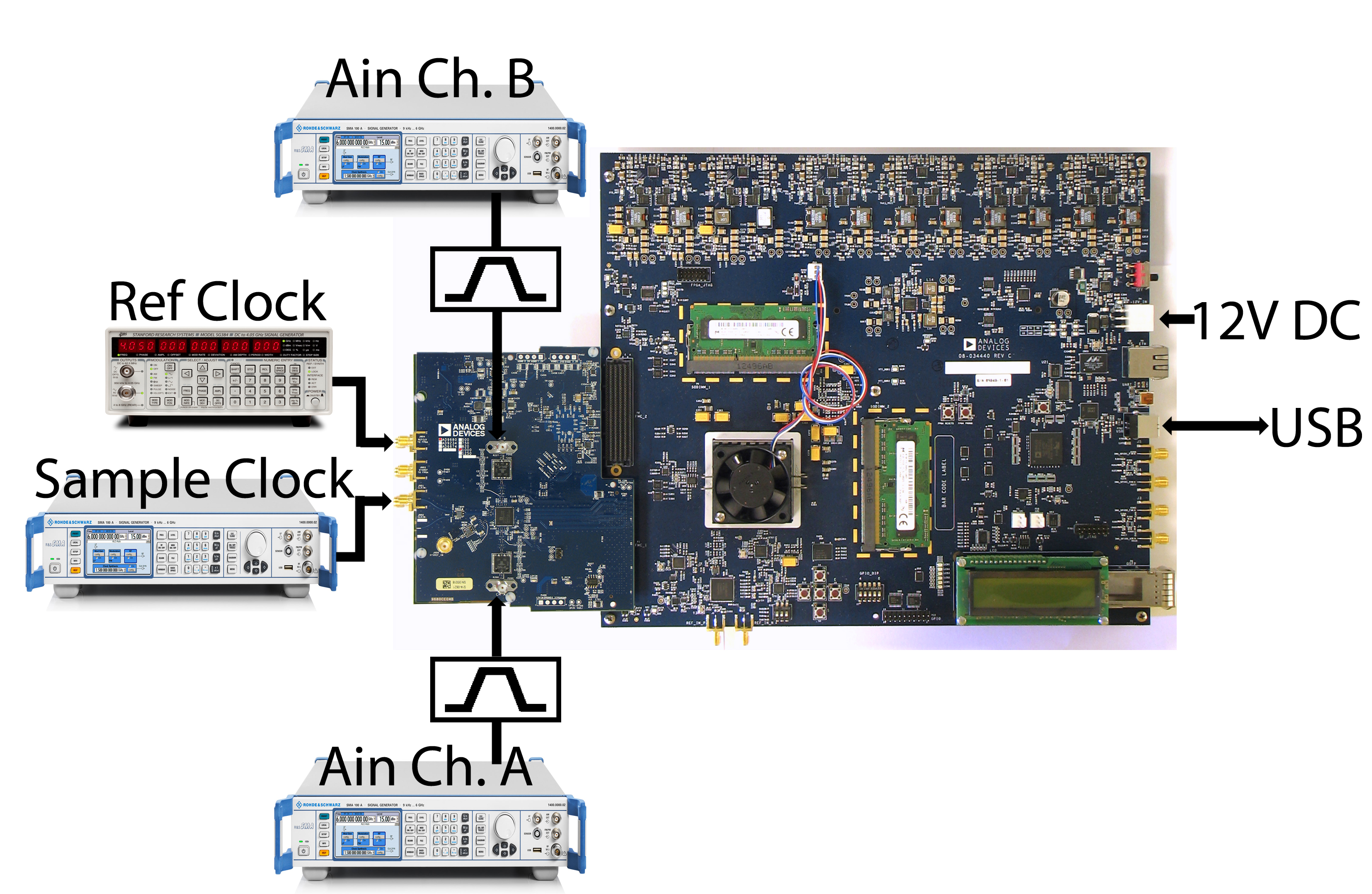
Connect the evaluation board to the
ADS7-V2EBZ/
ADS7-V1EBZ data capture board, as shown in Figures 1a and 1b.
Connect one 12V, 6.5A switching power supply (such as the CENB1080A1251F01 supplied) to P4 on the
ADS7-V2EBZ/
ADS7-V1EBZ board. Connect the Standard-B
USB port of the
ADS7-V2EBZ/
ADS7-V1EBZ board to the PC with the supplied
USB cable.
-
-
If the Device Manager does not show the
ADS7-V2EBZ/
ADS7-V1EBZ listed, unplug all
USB devices from the PC, uninstall and re-install SPIController and VisualAnalog and restart the hardware setup from step 1.
On the ADC evaluation board, provide a clean, low jitter 750MHz clock source to connector J801 and set the amplitude to 14dBm. This is the ADC Sample Clock.
On the ADC evaluation board, provide a clean, low jitter clock source to connector J804 and set the amplitude to 10dBm. This is the Reference Clock for the gigabit transceivers in the FPGA. The REFCLK frequency can be calculated using the following empirical formulae:
*f_{out}/L") bps/lane, where
bps/lane, where
 (Default Nprime = 16)
On the ADC evaluation board, use a clean signal generator with low phase noise to provide an input signal for channel A to P200. Use a shielded, RG-58, 50 Ω coaxial cable to connect the signal generator output to the ADC Evaluation Board. For best results, use a narrow-band, band-pass filter with 50 Ω terminations and an appropriate center frequency. (
ADI uses TTE, Allen Avionics, and
K & L band-pass filters.)
On the ADC evaluation board, use a clean signal generator with low phase noise to provide an input signal for channel B to P202. Use a shielded, RG-58, 50 Ω coaxial cable to connect the signal generator output to the ADC Evaluation Board. For best results, use a narrow-band, band-pass filter with 50 Ω terminations and an appropriate center frequency. (
ADI uses TTE, Allen Avionics, and
K & L band-pass filters.)
Software Setup
ACE Plugin currently supporting only Nprime = 16 and capture board ADS7-V2EBZ.
Download and install
ACE if it is not already installed.
The AD6674 ACE plug-in can be found under the
AD6674 Evaluation Board Software Section, or through ACE's Plug-In Manager (Tools → Manage Plug-Ins).
Tip: Some browsers (Such as Internet Explorer) may save the file as a .zip file instead of an .acezip file. If this happens, simply download and rename the file with an .acezip file extension.
Once the .acezip file has been downloaded from the Analog Devices website, right click on it and install the plug-in, or double click to install.
Click Start → All Programs → Analog Devices → ACE → ACE
The AD6674 plug-in should appear as in Figure 5 if installed correctly.
} Figure 5. ACE's AD6674 Plug-in
If the AD6674 plug-in does not appear, or no board is detected, make sure the ADS7-V2 is powered on and the evaluation board is properly connected. Make sure that ACE has been updated to the most recent version and the necessary plug-ins have been installed.
Note: Differences may occur between ACE plug-in versions, including the version number seen in Figure 7 above or components in any of the other images below - however, these will not affect the performance of the part, nor the fundamental features described in this user guide.
Double click on the plug-in to open it. This will open the AD6674 Board View.
 Figure 6. AD6674 Board View
Note: ACE will automatically program the FPGA (FPGA_DONE LED should be lit up) and load the default full bandwidth configuration.
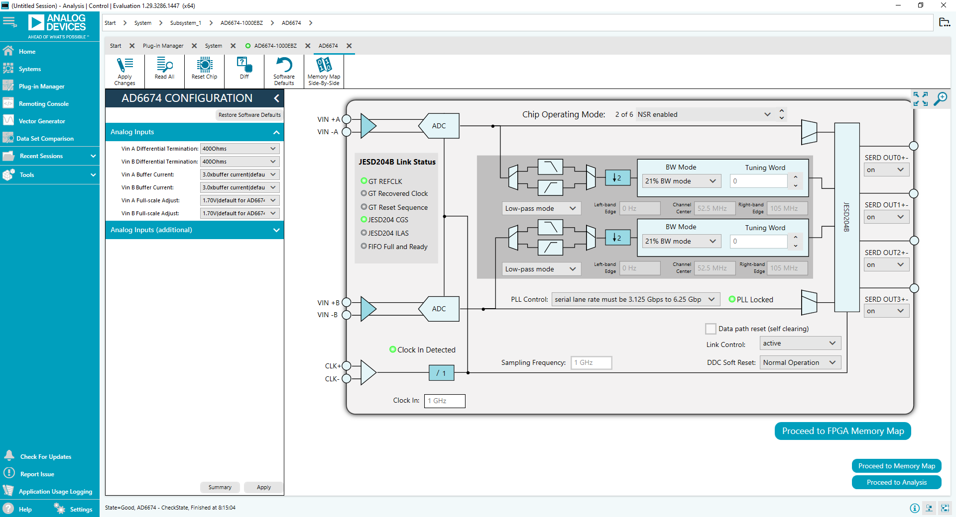
Double click on the blue AD6674 chip (in the middle of the board) to open up the Chip View.
 Figure 7. AD6674 Chip View
Visual Analog & SPI Controller Setup
Visual Analog & SPI Controller Setup
Visual Analog Setup
Click Start

All Programs
Analog Devices
VisualAnalog
VisualAnalog
On the VisualAnalog “New Canvas” window, click
ADCDualAD6674 
Figure 8. Selecting the AD6674 canvas
At this point, VisualAnalog will automatically detect the evaluation board and the FPGA data capture board and ask if it can program the FPGA with the appropriate bin file. This is shown in Figure 9.

If VisualAnalog opens with a collapsed view, click on the “Expand Display” icon (see figure 10)

Figure 10. Expanding Display in VA
Click the
Settings button in the
ADC Data Capture block as shown in Figure 11

Figure 11. Changing the ADC Capture Settings
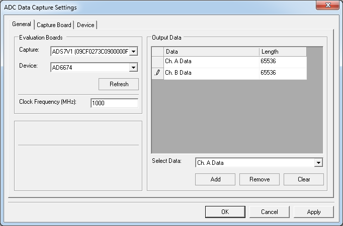
On the
General tab make sure the clock frequency is set to
750MHz (or other clock frequency). The FFT capture length may be changed to 131072 (128k) or 262144 (256k) per channel. The
ADS7-V2 and
ADS7-V1 FPGA software supports up to 2M FFT capture (1M per channel)
Figure 12. Setting the clock frequency and Capture length
If the board did not Auto-program click on the
Capture Board tab and browse to the
ad9680_ads7v1.bin or the
ad9680_ads7v2.bin file depending on which data capture board is being used. Click the
Program button. The
FPGA_DONE LED should illuminate on the
ADS7-V1 board indicating that the FPGA has been correctly programmed.
On the Device tab. Make sure that Enable Alternate REFCLK option is unchecked.
Click OK
SPI Controller Setup
Click Start
All Programs
Analog Devices
SPIController
SPIController
Select the appropriate configuration file when prompted.
In the
Global tab, under the
Generic Read/Write section, write 0x81 to register 0x000. This issues a Soft reset for the DUT.
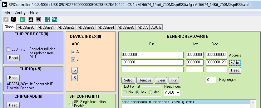
Figure 13. Sending a Soft Reset to the AD6674
The JESD204B quick configuration and Lane Rate registers are available in the
ADCBase3 tab. Set the Lane Rate setting register 0x56E to
Low Lane Rate Mode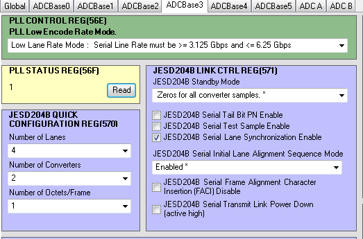
Figure 14. Setting the JESD204B Lane Rate
Set the JESD204B Quick Configuration register 0x570. For 1000MSPS operation with with default conditions (
Noise Shaped Requantizer (NSR) Mode), the values for
L.M.F are
4.2.1
Figure 15. Setting the JESD204B Quick Configuration Register
After the quick configuration setting is completed, the
PLL Lock Detect register 0x56F will read 0x80 to denote a lock. The SPIController interface will show a “1” to denote a lock.
Toggle the JESD204B link by checking and then unchecking the JESD204B Serial Transmit Power Down box
Individual Channel control for
ADC A and
ADC B are done using the Device Index Register (0x008) in the Global tab.

Figure 16. Device Index for ADC Channel A and Channel B
Under ADC A and ADC B tabs the options for Channel A and B are listed. Default settings have been programmed to ensure optimal performance for the input bandwidth and sample rate. Only the following options need to be operated with:
Chip Configuration Register (2): This option allows the channel to be powered on
Buffer Current Setting (18): This option allows the buffer current to change to enable better harmonic performance at different frequencies. At high analog input frequencies, the buffer current may need to be increased to optimize harmonic distortion performance (HD2, HD3). Keep in mind that at high frequencies, the performance is also jitter limited. So increasing the buffer currents may lead to diminishing returns with higher power consumption. Refer to the datasheet to understand the relationship between IAVDD3 and Buffer Current Setting.
Analog Input Differential Termination (16): This sets the input termination. Recommended settings are 500, 200, 100, 50 ohms. At lower termination settings, the harmonic distortion performance may show improvement, but the analog input signal amplitude will be reduced.
Input Full Scale Range (25): At high input frequencies, in order to preserve the linearity of the input buffer, it may be beneficial to reduce the input full-scale range in order to get more harmonic distortion performance. This in turn may negatively affect the SNR of the ADC.
Sample Configuration 1: NSR Mode
The default Chip Application Mode for the AD6674-750/AD6674-1000 is NSR with a chip decimation ratio of 2 (the AD6674-500 also defaults to NSR mode but with decimation disabled).
Under Initial Configuration at board view, set the following configuration below:
-
Decimate/2: True
Bandwidth Mode: 21%
Lane (L): 4
-
Octets per Frame (F): 1
Bits per Sample (N'):
16
 Figure 17. Chip Settings
Click
Apply to apply the chip settings. Set the
reference clock to
187.5 MHz to match these settings and click AD6674 to be directed to chip view.
Note: ACE will automatically load the default NSR mode configuration and can skip to step 6 to proceed to Analysis tab to capture data.
Click
Apply at
AD6674 Configuration, and then chip view will update to reflect all the changes made. If any changes are made, the chip can be read by clicking the
Read All button.

Figure 18. Read All Button
Issue a
Data Path Reset to the AD6674 by clicking its checkbox and then
Apply Changes. The data path reset bit will automatically self-clear.

Figure 19. Data Path Reset
If the
PLL Locked indicator lights up, you can reset it by powering down the JESD link using the
Link Control dropdown box, and clicking
Apply Changes.

Figure 20. PLL Lock, Link Power Down
Enable the
Link Control again and
Apply Changes.

Figure 21. PLL Lock, Link Enable
Click
Proceed to Analysis. This is ACE's Analysis tool for the data from the ADC, displaying both sample plots (Waveform) and FFTs. Click on
FFT and
Run Once to capture once.

Figure 22. Display FFTs and Run once
Tip: Capturing data using another program (
e.g. VisualAnalog, proprietary code, etc.) while using ACE concurrently may cause errors in ACE's data capture. If this occurs, the best solution is to restart the evaluation boards and work solely via ACE, or to setup the part in ACE then capture solely in the other program.
Channel A and
Channel B can be selected individually to display their
FFTs. A successful capture is shown below, with a 75
MHz signal inputted at on both Channel A and B. Adjust the amplitude of the input signal so that the fundamental is at the desired level. NSR imposes a ~3dB loss in the signal but does not impact the dynamic range. A -1.0
dBFS input signal will show as -4.0
dBFS in the FFT.

Figure 23. Example Data Capture to Channel B
To save the FFT plot, click on Export button at Analysis Results tab and save it to a location of choice.
Visual Analog & SPI Controller Configuration
Visual Analog & SPI Controller Configuration
SPI Controller Configuration
 Figure 24. Default Application Mode - NSR/Decimation by 2
The NSR mode settings are configured in the ADCA and ADCB tabs. The NSR defaults to 21% bandwidth mode with a tuning word of 0. Decimate by 2 is enabled by default also on the AD6674-750 and AD6674-1000 (and cannot be disabled in NSR mode).

Figure 25. Channel A and Channel B NSR Settings
Visual Analog Configuration
The first item to configure in Visual Analog is the input clock frequency. This is the frequency of the input clock and NOT the decimated sample rate (if using decimation). Click in the ADC Data Capture block to open the settings. In this example, 750MHz is the input clock frequency.

Figure 26. AD6674-750 FFT Data Capture Settings
In order to obtain an FFT with NSR enabled, Visual Analog must be configured correctly. Click on the settings button on the FFT Analysis block and configure the settings in Visual Analog to match the NSR settings that have been programmed into the AD6674. Under Advanced Calculation, click the Enable box, select AD6674 NSR, and then select the appropriate bandwidth mode and tuning word. Make sure to set the Bandwidth to match the mode. When finished, click the Apply button and then the OK button to apply the settings.
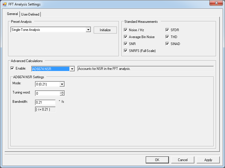
Figure 27. AD6674-750 FFT Analysis NSR Settings
In this example, with an input clock of 750MHz, the output sample rate is 375MSPS. The default JESD204B lane configuration is 4.2.1 (L.
M.F). The required REFCLK frequency is 187.5MHz (refer to step 7 in the section “Configuring the Board”).
Click the Run button in Visual Analog and you should see the capture data similar to the plot below.

Figure 28. AD6674-750 FFT with NSR Enabled
Adjust the amplitude of the input signal so that the fundamental is at the desired level. (Examine the
Fund Power reading in the left panel of the VisualAnalog FFT window.) NSR imposes a ~3dB loss in the signal, but does not impact the dynamic range. A -1.0
dBFS input signal will show as -4.0
dBFS in the FFT in Visual Analog.
To save the FFT plot do the following
Click on the Float Form button in the FFT window
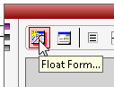
Figure 29. Floating the FFT window
Click on File
Save Form As button and save it to a location of choice
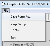
Figure 30. Saving the FFT
Sample Configuration 2: VDR Mode
Under Initial Configuration at board view, set the following configuration below:
Click
Apply to apply the chip settings. Set the
reference clock to
375 MHz to match these settings and click AD6674 to be directed to chip view.
Note: ACE will automatically load the initialization sequence after applying initial configurations.
In the chip view, set
Tuning Word to
0 and click
Apply at
AD6674 Configuration. Then chip view will update to reflect all the changes made. If any changes are made, the chip can be read by clicking the
Read All button.

Figure 32. Read All Button
Issue a
Data Path Reset to the AD6674 by clicking its checkbox and then
Apply Changes. The data path reset bit will automatically self-clear.

Figure 33. Data Path Reset
If the
PLL Locked indicator lights up, you can reset it by powering down the JESD link using the
Link Control dropdown box, and clicking
Apply Changes.

Figure 34. PLL Lock, Link Power Down
Enable the
Link Control again and
Apply Changes.

Figure 35. PLL Lock, Link Enable
Click
Proceed to Analysis. This is ACE's Analysis tool for the data from the ADC, displaying both sample plots (Waveform) and FFTs. Click on
FFT and
Run Once to capture once.
Figure 36. Display FFTs and Run once
Tip: Capturing data using another program (
e.g. VisualAnalog, proprietary code, etc.) while using ACE concurrently may cause errors in ACE's data capture. If this occurs, the best solution is to restart the evaluation boards and work solely via ACE, or to setup the part in ACE then capture solely in the other program.
Channel A and
Channel B can be selected individually to display their
FFTs. A successful capture is shown below, with a 75MHz signal inputted at on both Channel A and B. Adjust the amplitude of the input signal so that the fundamental is at -1.0
dBFS.

Figure 37. Example Data Capture to Channel A and B
To save the FFT plot, click on Export button at Analysis Results tab and save it to a location of choice.
Visual Analog & SPI Controller Configuration
Visual Analog & SPI Controller Configuration
SPI Controller Configuration
The settings in the ADCBase0 tab must be changed to configure the AD6674 into VDR mode. To set up the AD6674 for VDR mode change the Chip Application Mode in register 0x200 to Variable Dynamic Range (VDR) Mode and set the Chip Decimation Ratio in register 0x201 to Full Sample Rate.

Figure 38. Set Application Mode to VDR
The VDR mode tuning word can be configured in the ADC A and ADC B tabs. VDR defaults to 25% bandwidth complex mode with a tuning word of 0. The tuning word can be changed using the VDR Tuner Frequency selection (register 0x434). See the AD6674 data sheet for more details on the available bandwidth modes and tuning words.

Figure 39. Channel A and Channel B VDR Settings
Using the default lane configuration in the AD6674 (L.
M.F = 4.2.1) the JESD204B lane rate will be 7.5
Gbps which means the
PLL must be set to Maximum Lane Rate Mode (0x56E) int he ADCBase3 tab in SPIController.

Figure 40. PLL Encode Settings
Visual Analog Configuration
The first item to configure in Visual Analog is the input clock frequency. This is the frequency of the input clock and NOT the decimated sample rate (if using decimation). Click in the ADC Data Capture block to open the settings. In this example, 750MHz is the input clock frequency.
Figure 41. AD6674-750 FFT Data Capture Settings
In this example, with an input clock of 750MHz, the output sample rate is 750MSPS. The default JESD204B lane configuration is 4.2.1 (L.
M.F). The required REFCLK frequency is 375MHz (refer to step 7 in the section “Configuring the Board”).
Click the Run button in Visual Analog and you should see the capture data similar to the plot below.

Figure 42. AD6674-750 FFT with VDR Enabled
Adjust the amplitude of the input signal so that the fundamental is at the desired level. (Examine the
Fund Power reading in the left panel of the VisualAnalog FFT window.) VDR imposes no loss on the input signal so a -1.0
dBFS input signal will show as -1.0
dBFS in the FFT in Visual Analog.
To save the FFT plot do the following
Click on the Float Form button in the FFT window
Figure 43. Floating the FFT window
Click on File
Save Form As button and save it to a location of choice
Figure 44. Saving the FFT
Sample Configuration 2.1: VDR Mode - Use Control Bits as VDR Punish Bits and the VDR High/Low Resolution Bit
Logic Analyzer not supported on AD6674 ACE Plugin. Converter Control bit 0, 1, and 2 (0x559 and 0x55A) and Number of control bits per sample (0x58F) can be configured thru ACE by accessing Chip's Memory Map. For Logic Analyzer, Visual Analog can be used for data capture.
Visual Analog & SPI Controller Configuration
Visual Analog & SPI Controller Configuration
SPI Controller Configuration
The first step, go to the ADCBase2 tab in SPIController to set up the control bits to select the VDR indicator bits. In this example Control Bit 2 is set to VDR Punish Bit 1, Control Bit 1 is set to VDR Punish Bit 0, and Control Bit 0 is set to the VDR High/Low resolution bit. (Similarly, the control bits may be set up to function as Overrange, Signal Monitor (SMON), or Fast Detect (FD) indicators.)
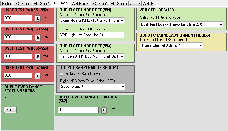
Figure 45. SPIController ADCBase2 Settings for VDR Indicators in the Control Bits
Next go to the ADCBase4 tab to set up the control bits to select the VDR indicator bits. In this example three control bits are sent per sample. In order to accommodate three control bits, the converter resolution (N) must be set to 13 bits (there are 16 available bits in the JESD204B data word and if three are used for control bits there are 13 bits available for the converter sample - in this example this means there will only be 13 bits available instead of the 14 bits of converter resolution.
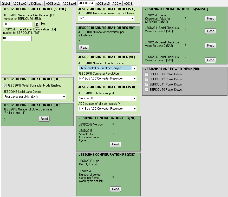
Figure 46. SPIController ADCBase4 Settings for Enabling the Control Bits
Visual Analog Configuration
The first step is to open a new Logic canvas in VisualAnalog. In the Logic canvas configure the Input Formatter to set the Resolution to 16 bits and the Alignment to 18 bits. This will create the space such that all three control bits can be visible in the Logic canvas.

Figure 47. Input Formatter Settings for VDR Indicators in the Control Bits
Next configure the Logic Analysis block for the data alignement. Set the High Bit to 15 and the low bit to 0. This will align the canvas such that all three control bits can be visible in the Logic canvas.

Figure 48. Logic Analysis Settings for Bit Alignment
These settings will create the space in the Logic Canvas display so that all three control bits available in the JESD204B data stream will be visible. (While the example here is for VDR the control bits may be set up to function as Overrange, Signal Monitor (SMON), or Fast Detect (FD) indicators and can be viewed in the output data in a similar manner.)

Figure 49. Logic Canvas Display Showing Available Control Bits
Once a signal is input that will trigger VDR to operate the VDR punish bits [1:0] and the VDR High/Low resolution bit can be seen in the Logic Canvas display. In this case control bit 2 is VDR punish bit 1, control bit 1 is VDR punish bit 0, and control bit 0 is the VDR High/Low resolution bit.
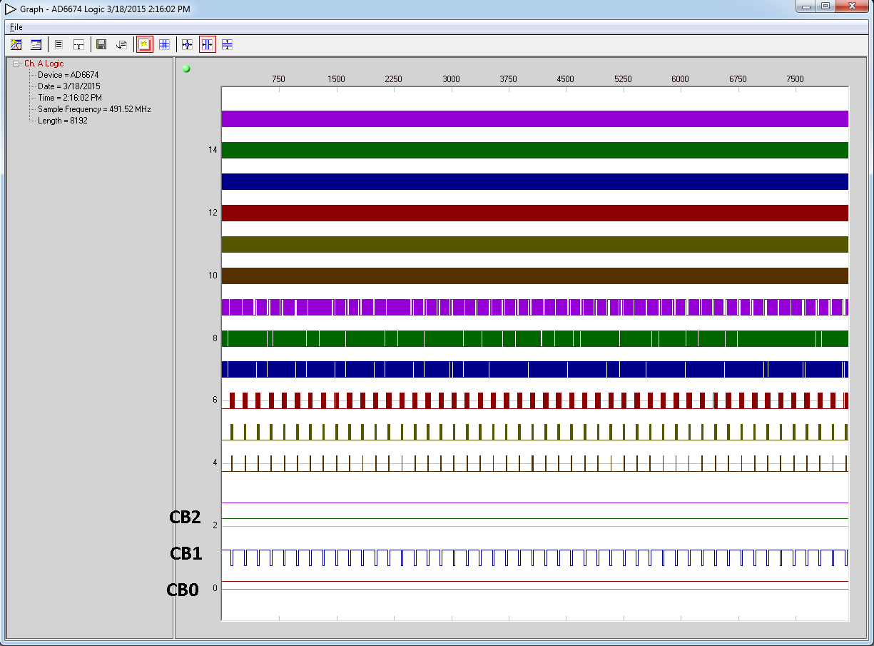
Figure 50. Logic Canvas Display Showing Control Bits [2:0] Indicating VDR Status
Note that the data alignment from the FPGA to VisualAnalog will fill in the control bits starting from the
LSB location in the Logic Canvas display. In this example data bit two is control bit 2, data bit 1 is control bit 1, and data bit 0 is control bit 0. If only using control bit 2 then this would reside in the data bit 0 location in the Logic Canvas display.

Figure 51. Logic Canvas Display Showing Control Bit 2 Only
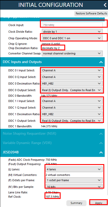
Sample Configuration 3: 2 ADCs, 2DDCs, Real Mode Decimate by 2
Under Initial Configuration at board view, set the following configuration below:
-
Chip Operating Mode: DDC 0 and DDC 1 on
DDC 0 and DDC 1 I/Q Input Select: Channel A
DDC 0 and DDC 1 Decimation Ratio: HB1_HB2
DDC 0 and DDC 1 Output Select: Real(I) Output Only.
Lane (L): 4
-
Octets per Frame (F): 1
Bits per Sample (N'):
16
 Figure 52. Chip Settings
Click
Apply to apply the chip settings. Set the
reference clock to
187.5 MHz to match these settings and click AD6674 to be directed to chip view.
Note: ACE will automatically load the initialization sequence after applying initial configurations.
In the chip view, set the following additional configuration to DDC 0 and DDC 1 by selecting the dropdown:
-
IF Mode: Variable IF Mode
-
Mixer Select: Real Mixer
Click
Apply at
AD6674 Configuration. Then chip view will update to reflect all the changes made. If any changes are made, the chip can be read by clicking the
Read All button.

Figure 53. Read All Button
After applying DDC settings, set
DDC Soft Reset to
DDC Held in Reset and
Apply Changes, then return it back to
Normal Operation and
Apply Changes.

Figure 54. DDC Soft Reset
Issue a
Data Path Reset to the AD6674 by clicking its checkbox and then
Apply Changes. The data path reset bit will automatically self-clear.

Figure 55. Data Path Reset
If the
PLL Locked indicator lights up, you can reset it by powering down the JESD link using the
Link Control dropdown box, and clicking
Apply Changes.

Figure 56. PLL Lock, Link Power Down
Enable the
Link Control again and
Apply Changes.

Figure 57. PLL Lock, Link Enable
Click
Proceed to Analysis. This is ACE's Analysis tool for the data from the ADC, displaying both sample plots (Waveform) and FFTs. Click on
FFT and
Run Once to capture once.
Figure 58. Display FFTs and Run once
Tip: Capturing data using another program (
e.g. VisualAnalog, proprietary code, etc.) while using ACE concurrently may cause errors in ACE's data capture. If this occurs, the best solution is to restart the evaluation boards and work solely via ACE, or to setup the part in ACE then capture solely in the other program.
Channel A and
Channel B can be selected individually to display their
FFTs. A successful capture is shown below, with a 75MHz signal inputted at on both Channel A and B. Adjust the amplitude of the input signal so that the fundamental is at -1.0
dBFS.

Figure 59. Example Data Capture to Channel A and B
To save the FFT plot, click on Export button at Analysis Results tab and save it to a location of choice.
Visual Analog & SPI Controller Configuration
Visual Analog & SPI Controller Configuration
SPI Controller Configuration
The settings in the ADCBase0 tab must be changed to configure the AD6674 to use the DDCs. In this example the AD6674 is set up to use two DDCs (one per ADC channel) with real outputs and a decimation ratio of two. Set the Chip Application Mode in register 0x200 to Two Digital Down Converters and select the Only Real (I) Selected checkbox. Set the Chip Decimation Ratio in register 0x201 to Decimate by 2 Ratio.
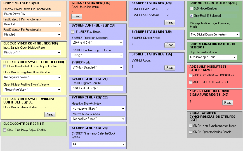
Figure 60. Set Application Mode to 2 DDCs Real Mode Decimate by 2
The DDC settings must be configured in ADCBase1, but first, the tuning step, translation frequency, and DDC Phase Increment must be calculated.
The tuning step is equal to the output sample rate divided by 4096.
tuning step = 375MSPS/4096 = 91552.734375
The translation frequency is equal to the output sample rate divided by 4*(decimation ratio).
translation frequency = 375MSPS/(4*2) = 46875000
The DDC Phase Increment is equal to the translation frequency divided by the tuning step.
DDC Phase Increment = 46875000/91552.734375 = 512
Under DDCO CTRL and DDC1 CTRL in the ADCBase1 tab configure the DDCs to select 6dB Gain, Variable IF Mode, Real(I) Decimate by 2 Filter Selection, Both Input Sample Selections to Channel A for DDC0 and Channel B for DDC1, and the DDC Phase Increment to the calculated value of 512
After changing DDC selections, perform a soft reset of the DDCs by checking and unchecking the box for DDC Soft Reset under the DDC Synchronization CTRL Reg (300).
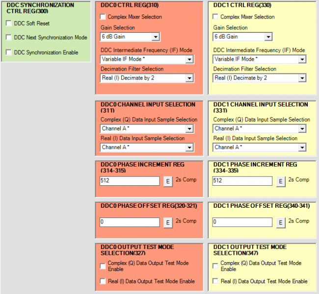
Figure 61. Channel A and Channel B DDC Settings
Using the default lane configuration in the AD6674 (L.
M.F = 4.2.1) the JESD204B lane rate will be 3.75Gbps which means that the
PLL needs to be set to Low Lane Rate Mode (0x56E) in the ADCBase3 tab in SPIController. This is the default setting so no change is needed.
Visual Analog Configuration
The first item to configure in Visual Analog is the input clock frequency. This is the frequency of the input clock and NOT the decimated sample rate (if using decimation). Click in the ADC Data Capture block to open the settings. In this example, 750MHz is the input clock frequency. In addition, the DDC data must be selected under the Output Data section. DDC0 and DDC1 are being used in the AD6674 so this must be selected under the ADC Data Capture Settings.
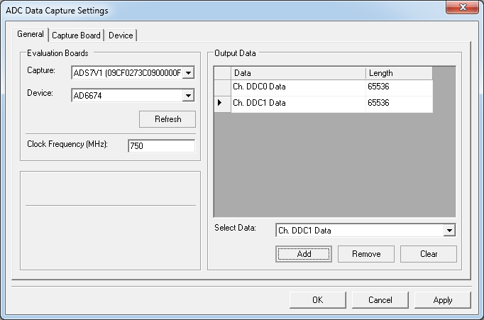
Figure 62. AD6674-750 FFT Data Capture Settings
In this example, with an input clock of 750MHz, the output sample rate is 375MSPS. The default JESD204B lane configuration is 4.2.1 (L.
M.F). The required REFCLK frequency is 187.5MHz (refer to step 7 in the section “Configuring the Board”).
Click the Run button in Visual Analog and you should see the capture data similar to the plot below.

Figure 63. AD6674-750 FFT with 2 DDCs in Real Mode with Dec2 Enabled
Adjust the amplitude of the input signal so that the fundamental is at the desired level. (Examine the
Fund Power reading in the left panel of the VisualAnalog FFT window.) Real DDC operation imposes ~0.7
dB loss on the input signal but does not impact the dynamic range. A -1.0
dBFS input signal will show as -1.7
dBFS in the FFT in Visual Analog.
To save the FFT plot do the following
Click on the Float Form button in the FFT window
Figure 64. Floating the FFT window
Click on File
Save Form As button and save it to a location of choice
Figure 65. Saving the FFT
Sample Configuration 4: 2 ADCs, 1DDC, Complex ZIF Mode Decimate by 2
Visual Analog & SPI Controller Configuration
Visual Analog & SPI Controller Configuration
SPI Controller Configuration
The settings in the ADCBase0 tab must be changed to configure the AD6674 to use the DDC. In this example the AD6674 will be set up to use one DDCs with a complex ZIF output (NCO bypassed) and a decimation ration of two. Set the Chip Application Mode in register 0x200 to One Digital Down Converter and make sure the Only Real (I) Selected checkbox is
NOT checked. Set the Chip Decimation Ratio in register 0x201 to Decimate by 2 Ratio.

Figure 74. Set Application Mode to 1 DDC Complex ZIF Mode Decimate by 2
The DDC settings must be configured under DDCO CTRL in the ADCBase1 tab configure the DDC to select Complex Mixer Selection, 0 Hz IF Mode, Decimate by 2 Filter Selection, Real (I) Input Sample Selection to Channel A for DDC0, and Complex (Q) Input Sample Selection to Channel B.
After changing DDC selections, perform a soft reset of the DDCs by checking and unchecking the box for DDC Soft Reset under the DDC Synchronization CTRL Reg (300).
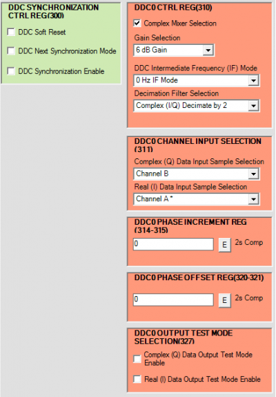
Figure 42. DDC Settings for Complex ZIF Mode
Using the default lane configuration in the AD6674 (L.
M.F = 4.2.1) the JESD204B lane rate will be 3.75Gbps which means that the
PLL needs to be set to Low Lane Rate Mode (0x56E) in the ADCBase3 tab in SPIController. This is the default setting so no change is needed.
Visual Analog Configuration
The first item to configure in Visual Analog is the input clock frequency. This is the frequency of the input clock and NOT the decimated sample rate (if using decimation). Click in the ADC Data Capture block to open the settings. In this example, 750MHz is the input clock frequency. In addition, the DDC data must be selected under the Output Data section. DDC0 is being used in the AD6674 so this must be selected under the ADC Data Capture Settings.
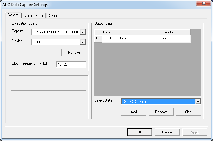
Figure 75. AD6674-750 FFT Data Capture Settings
In this example, with an input clock of 750MHz, the output sample rate is 750MSPS. The default JESD204B lane configuration is 4.2.1 (L.
M.F). The output sample rate is 375MSPS and the required REFCLK frequency is 187.5MHz (refer to step 7 in the section “Configuring the Board”).
In order to exclude the image frequency from the SFDR measurements, configure Visual Analog to remove the image from its calculations. This is done under the FFT Analysis settings. Under the User-Defined tab add a new row by clicking Add. Name it ‘Image’. Use a symbol such as the # and set the Freq to ‘-fund’. Set the Single-Side Band to 3 Bins and set it as ‘Spur, Exclude’. Once done, select the row, and then hit the Move Up button to place this new row just below the row with Fund.
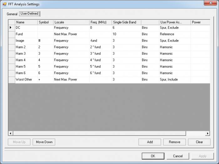
Figure 76. AD6674-750 FFT Analysis Settings for Complex Image
Click the Run button in Visual Analog and you should see the capture data similar to the plot below.

Figure 77. AD6674-750 FFT with 1 DDC in Complex ZIF Mode with Dec2 Enabled
Adjust the amplitude of the input signal so that the fundamental is at the desired level. (Examine the “Fund Power” reading in the left panel of the VisualAnalog FFT window.) Complex DDC operation imposes ~1dB loss in the signal, but does not impact the dynamic range. A -1dBFS input signal will show as -2dBFS in Visual Analog.
To save the FFT plot do the following
Click on the Float Form button in the FFT window
Figure 78. Floating the FFT window
Click on File
Save Form As button and save it to a location of choice
Figure 79. Saving the FFT
Troubleshooting Tips
Evaluation board is not functioning properly
Evaluation board is not communicating with the ADS7-V2 / No SPI communication
Make sure that the FPGA on the ADS7-V2 has been programmed - a lit LED DS15 (FPGA_DONE) on the top of the ADS7-V2 and a powered fan are good indicators of the FPGA being programmed.
Check the common mode voltage on the JESD204B traces. On the evaluation board, the common mode voltage should be roughly two-thirds of DRVDD_1. On the ADS7-V2, the common mode voltage should be around 1.2 volts.
To test
SPI operation, attempt to both read and write to register 0x00A (Scratch Pad) using ACE's Register Debugger (Tools → Register Debugger). This register is an open register available for testing memory reads and writes. If the register reads back the same value written to it,
SPI is operational.
All registers reading back as either all ones or all zeros (
i.e., 0xFF or 0x00) may indicate no
SPI communication.
Register 0x000 (
SPI Configuration A) reading back 0x81 in ACE may indicate no
SPI communication as a result of the FPGA on the ADS7-V2 not being programmed.
ACE software fails to capture date
Ensure that the board is functioning properly and that
SPI communication is successful - see previous troubleshooting tips.
Check the Clock Status register 0x011C to see if the input sample clock is being detected. 0x01 indicates detection, 0x00 indicates no clock detected. Check the signal generator input on connector J801. Try checking the common mode voltage on the clock pins, which should be roughly two-thirds of AVDD_1. Try placing a differential oscilloscope probe on the clock pins to see if the clock signal is reaching the chip.
Check the
PLL Locked indicator (see figure 23) or register 0x056F (
PLL Status). If the light in the plugin chip view is green or if the register reads back 0x80, the
PLL is locked. If it is not locked:
Check the clock being input to connector J801.
Check the JESD204B settings under the Initial Configuration. Reference the
AD6674 datasheet for supported lane options.
Check the Reference Clock and make sure it matches your JESD settings.
Make sure P100 (Power Down / Standby Jumper) is not jumped.
FFT plot appears abnormal
If you see a normal noise floor when you disconnect the signal generator from the analog input, be sure you are not overdriving the ADC. Reduce input level if necessary.
In VisualAnalog, Click on the Settings button in the Input Formatter block. Check that Number Format is set to the correct encoding (twos compliment by default). Repeat for the other channel.
Issue a Data Path Soft Reset to DUT.
The FFT plot appears normal, but performance is poor.
Make sure you are using the appropriate band-pass filter on the analog input.
Make sure the signal generators for the clock and the analog input are clean (low phase noise).
If you are using non-coherent sampling, change the analog input frequency slightly, or use coherent frequencies.
Make sure the
SPI config file matches the product being evaluated.
The FFT window remains blank after the Run button is clicked
VisualAnalog indicates that the “FIFO capture timed out” or “FIFO not ready for read back”
VisualAnalog displays a blank FFT when the RUN button is clicked
resources/eval/ad6674-1000ebz.txt · Last modified: 18 Apr 2024 01:54 by
Deferson Romero