


This version (23 Dec 2021 17:31) was approved by Jordyn Ansari.The Previously approved version (01 Dec 2021 10:00) is available.
Table of Contents
ADA4254 Reference Manual
General Information
The ADA4254 reference manual should be used in conjunction with the device datasheet and is intended for use as a guide to setting up the ADA4254 for a user-specific application. It describes user-programmable registers and the data signal path for the ADA4254 to assist in determining which internal components require programming. Several examples are provided to assist with this task.
Digital Interface Overview
The ADA4254 features a 4-wire SPI interface which operates in SPI Mode 0 when CS is low. The falling edge of SCLK is the drive edge and the rising edge of SCLK is the sample edge. In this mode, data is clocked out of the device on the falling (drive) edge of SCLK and data is clocked into the device on the rising (sample) edge. The ADA4254 SPI interface uses 16-bit instructions with each instruction including a single read/write bit, seven address bits and eight data bits. The drive and sample edges of SCLK are shown in Figure 1.
 Figure 1. SCLK Edges in SPI Mode 0
Locked/Unlocked Reserved Bits
Some registers in the ADA4254 contain RESERVED bits that do not affect the operation of the device and are described as being either LOCKED or UNLOCKED. A RESERVED bit whose state can be changed (written to) is said to be UNLOCKED whereas LOCKED bits remain in their default state (0x0). The user-accessible register map for the ADA4254, showing the distribution of RESERVED bits is shown in Figure 2.
| Reg Address | Name | Bit 7 | Bit 6 | Bit 5 | Bit 4 | Bit 3 | Bit 2 | Bit 1 | Bit 0 |
|---|---|---|---|---|---|---|---|---|---|
| 0x00 | Gain_Mux | G4 | G[3:0] | Reserved(UNLOCKED) | EXT_MUX[1:0] | ||||
| 0x01 | Reset | Reserved(LOCKED) | RST | ||||||
| 0x02 | SYNC_CNFG | Reserved(UNLOCKED) | CLK_OUT_SEL | Reserved(UNLOCKED) | SYNC_POL | Reserved(UNLOCKED) | SYNC[2:0] | ||
| 0x03 | DIGITAL_ERR | Reserved(LOCKED) | CAL_BUSY | SPI_CRC_ERR | SPI_RW_ERR | SPI_SCLK_CNT_ERR | Reserved(LOCKED) | MM_CRC_ERR | ROM_CRC_ERR |
| 0x04 | ANALOG_ERR | G_RST | POR_HV | Reserved(LOCKED) | WB_ERR | FAULT_INT | OUTPUT_ERR | INPUT_ERR | MUX_OVER_VOLT_ERR |
| 0x05 | GPIO_DATA | Reserved(LOCKED) | GPIO_DATA[6:0] | ||||||
| 0x06 | INPUT_MUX | Reserved(LOCKED) | SW_A1 | SW_A2 | SW_B1 | SW_B2 | SW_C1 | SW_C2 | SW_D12 |
| 0x07 | WB_DETECT | WB_G_RST_DIS | Reserved(UNLOCKED) | SW_F1 | SW_F2 | WB_CURRENT[1:0] | |||
| 0x08 | GPIO_DIR | Reserved(LOCKED) | GPIO_DIR[6:0] | ||||||
| 0x09 | SCS | Reserved(LOCKED) | SCS[6:0] | ||||||
| 0x0A | ANALOG_ERR_DIS | G_RST_DIS | POR_HV_DIS | Reserved(UNLOCKED) | WB_ERR_DIS | MUX_PROT_DIS | OUTPUT_ERR_DIS | INPUT_ERR_DIS | MUX_OVER_VOLT_ERR_DIS |
| 0x0B | DIGITAL_ERR_DIS | Reserved(UNLOCKED) | CAL_BUSY_DIS | SPI_CRC_ERR_DIS | SPI_RW_ERR_DIS | SPI_SCLK_CNT_ERR_DIS | M_CLK_CNT_ERR_DIS | MM_CRC_ERR_DIS | ROM_CRC_ERR_DIS |
| 0x0C | SF_CFG | Reserved(UNLOCKED) | INT_CLK_OUT | EXT_CLK_IN | FAULT_INT_OUT | CAL_BUSY_OUT | EXT_MUX_EN[1:0] | ||
| 0x0D | ERR_CFG | ERR_LATCH_DIS | Reserved(UNLOCKED) | ERR_DELAY[3:0] | |||||
| 0x0E | TEST_MUX | G5 | CAL_SEL | CAL_EN[1:0] | TEST_MUX[3:0] | ||||
| 0x0F | EX_CURRENT_CFG | EX_CURRENT_SEL[1:0] | Reserved(UNLOCKED) | EX_CURRENT[3:0] | |||||
| 0x10 | GAIN_CALx | Reserved(LOCKED) | GAIN_CAL_1[4:0] | ||||||
| 0x11 | Reserved(LOCKED) | GAIN_CAL_2[4:0] | |||||||
| 0x12 | Reserved(LOCKED) | GAIN_CAL_3[4:0] | |||||||
| 0x13 | Reserved(LOCKED) | GAIN_CAL_4[4:0] | |||||||
| 0x14 | Reserved(LOCKED) | GAIN_CAL_5[4:0] | |||||||
| 0x15 | Reserved(LOCKED) | GAIN_CAL_6[4:0] | |||||||
| 0x16 | Reserved(LOCKED) | GAIN_CAL_7[4:0] | |||||||
| 0x17 | Reserved(LOCKED) | GAIN_CAL_8[4:0] | |||||||
| 0x18 | Reserved(LOCKED) | GAIN_CAL_9[4:0] | |||||||
| 0x19 | Reserved(LOCKED) | GAIN_CAL_10[4:0] | |||||||
| 0x1A | Reserved(LOCKED) | GAIN_CAL_11[4:0] | |||||||
| 0x1B | Reserved(LOCKED) | GAIN_CAL_12[4:0] | |||||||
| 0x1C | Reserved(LOCKED) | GAIN_CAL_13[4:0] | |||||||
| 0x1D | Reserved(LOCKED) | GAIN_CAL_14[4:0] | |||||||
| 0x1E | Reserved(LOCKED) | GAIN_CAL_15[4:0] | |||||||
| 0x1F | Reserved(LOCKED) | GAIN_CAL_16[4:0] | |||||||
| 0x20 | Reserved(LOCKED) | GAIN_CAL_17[4:0] | |||||||
| 0x21 | Reserved(LOCKED) | GAIN_CAL_18[4:0] | |||||||
| 0x22 | Reserved(LOCKED) | GAIN_CAL_19[4:0] | |||||||
| 0x23 | Reserved(LOCKED) | GAIN_CAL_20[4:0] | |||||||
| 0x24 | Reserved(LOCKED) | GAIN_CAL_21[4:0] | |||||||
| 0x25 | Reserved(LOCKED) | GAIN_CAL_22[4:0] | |||||||
| 0x26 | Reserved(LOCKED) | GAIN_CAL_23[4:0] | |||||||
| 0x27 | Reserved(LOCKED) | GAIN_CAL_24[4:0] | |||||||
| 0x2A | TRIG_CAL | Reserved(UNLOCKED) | TRIG_CAL | ||||||
| 0x2E | M_CLK_CNT | M_CLK_CNT[7:0] | |||||||
| 0x2F | DIE_REV_ID | DIE_REV_ID[7:0] | |||||||
| 0x64 | PART_ID | PART_ID[39:32] | |||||||
| 0x65 | PART_ID[31:24] | ||||||||
| 0x66 | PART_ID[23:16] | ||||||||
| 0x67 | PART_ID[15:8] | ||||||||
| 0x65 | PART_ID[7:0] | ||||||||
GPIOs
The ADA4254 features 7 GPIOs for the LFCSP package and 5 GPIOs for the TSSOP package. These GPIOs may be configured to read a logic input or output a logic signal through the “GPIO Direction (GPIO_DIR) Register (0x08)”.
GPIO data can be read back in the “GPIO_DATA Register (0x05)”. When configured as an output, it reads back the forced data and when set as an input, the register samples the value on the input pin.
It is important to note that GPIO pins are configured as inputs by default because some functions require that a GPIO pin be first configured as an output.
GPIO Special Functions
GPIO0 to GPIO4 have their own Special Functions that can be enabled through “Special Function(SF_CFG) Register (0x0C)”. To use the special functions for GPIO0 through GPIO3, the GPIO pins must first be configured as outputs .
GPIO0 to GPIO1 (External Mux Controller)
A special function of GPIO0 to GPIO1 is to control an external multiplexer. When these GPIO pins are configured as outputs and the special function register bits are enabled, the pins match the settings of the first 2 bits in the “Gain and Mux Control (Gain_MUX) Register (0x00)”. This allows a user to change gain and mux settings using a single write to the register.
GPIO2 (Calibration Busy Output)
GPIO2 can be configured to output a calibration busy signal. This function is enabled using the CAL_BUSY_OUT bit in the SF_CFG Register (0x0C). The CAL_BUSY bit from the “Digital Error (DIGITAL_ERR) Register (0x03)” is output to GPIO2 when this special feature is enabled. This signal indicates that the ADA4254 is busy performing a calibration routine.
GPIO3 (Fault Interrupt Output)
GPIO3 can be used to output a fault interrupt signal from either the “Analog Error (ANALOG_ERR) Register (0x04)” or “Digital Error (DIGITAL_ERR) Register (0x03)”. The contents of these registers are logically ORed and the result is sent to the GPIO3 pin. This function is controlled using FAULT_INT_OUT Bit in the SF_CFG Register (0x0C).
GPIO4 (Clock Input or Output)
A special function of GPIO4 is that it can be used as an input or an output for the ADA4254's clocking scheme. When configured as an input and the “EXT_CLK_IN” control bit in the SF_CFG Register in enabled, the ADA4254 will accept an external clock ranging from 1MHz to 32MHz. However, if the clock frequency is greater than 1MHz, then its frequency must be divided back down to 1MHz using the Clock Synchronization Configuration (SYNC_CFG) Register's (0x02) Internal Clock Divider Value (SYNC) bits. The clock synchronization polarity is set using the SYNC_POL bits in the SYNC_CFG register. By configuring GPIO4 as an output and setting the Internal Oscillator Output (INT_CLK_OUT) to 1 from the SF_CFG register, the ADA4254 outputs either a 1MHz master clock or a 125kHz clock that is used by the zero drift amplifiers within the chip. The Clock Output Select (CLK_OUT_SEL) bit in the SYNC_CFG (0x02) register controls which clock is output to the pin.
When using an external clock with the ADA4254, it is important for it to have a frequency between 0.8MHz to 1.2MHz and a 50% duty cycle to ensure proper device operation. Clock signals with a higher frequency must be divided down to 1MHz.
Memory Map (MM)/Read-Only Memory (ROM) CRC Functionality
For added robustness, the ADA4254 performs a CRC check on its memory map and ROM.
MM/ROM CRC Calculation at Power-Up
A CRC calculation is performed on the default values of on-chip registers (MM) at power-up. Registers 0x03, 0x04 and 0x05 are excluded from this check because their contents change independently of SPI write operations. The result of the MM CRC calculation is stored as a “Golden” value. A CRC calculation is also performed on all fuse (ROM) registers and the result is stored as a separate “Golden” value. Sometime after the initial CRC is completed, the state machine begins running.
MM/ROM CRC Calculation at Periodic Intervals
A CRC on the MM registers is repeated periodically approximately every 512 μs, or once every period of the 1MHz internal oscillator (or state machine) clock divided by 512 (Figure 3). This time interval varies because the 1 MHz oscillator is specified to have a tolerance of ±20%. The MM CRC begins on the rising edge of the state machine clock, while the ROM CRC begins on the falling edge. Each “sub” state machine cycle consists of a CRC calculation of the current registers/fuses, followed by a comparison with the stored “Golden” value. If the calculated values differ to the “Golden values”, the MM CRC or ROM CRC error flags are set.
 Figure 3. CRC State Machine - High Level Operation
A MM CRC calculation lasts for 19 oscillator clock cycles (~19μs) while a ROM CRC calculation lasts for 32 oscillator clock cycles (~32μs). The comparison between the calculated CRC and the “Golden” value occurs on the oscillator clock edge which follows the end of the calculation. If the MM CRC or ROM CRC flags are disabled prior to the state machines starting, then a CRC is not performed.
Depending on the where it is in a cycle, the state machine looks for changes to the MM and for activity on the SPI - see “Detection of SPI Activity during MM CRC/ROM CRC State Machine Cycles”. If a change to the MM is detected, a new “Golden” value is calculated before it begins to calculate an updated CRC checksum using the current register values. If SPI activity (read or write) is detected during the MM CRC calculation, the state machine remains idle until the next state machine clock edge.
ROM CRC Error
Fuse values cannot be changed by a user so if a ROM CRC error occurs it is strongly recommended to reset or power-cycle the ADA4254. If the ROM CRC error does not clear, it is possible that the device has been permanently damaged.
MM CRC Error
If a MM CRC error occurs, this means that the stored “Golden” CRC value does not match the most recently calculated value. There are several reasons why this could occur. If a bit flips in a register over time, it causes the MM_CRC_ERR flag to be set. However, if the user writes to the part too quickly or while a CRC calculation is in progress, the state machine might not detect that the registers are changing.
Detection of SPI Activity During MM/ROM CRC State Machine Cycles
The ADA4254 uses Method 1 to detect SPI activity and force the state machine to the idle state. The ADA4254 uses Method 2 to detect changes to user registers and force a recalculation of the “Golden” value.
Method 1: SPI Activity During MM CRC Calculations
During the 19 oscillator clocks of the MM CRC calculation, the ADA4254 looks for SPI activity (read or write) from the first rising edge of SCLK after CSB goes low to when CSB goes high after a read/write operation. The signal that is active during this time is sampled using the internal oscillator clock (Figure 4). If this signal is sampled correctly, the state machine remains idle until the next edge of the state machine clock. Note that this does not trigger a recalculation of the “Golden” CRC value, and Method 2 must be used instead.
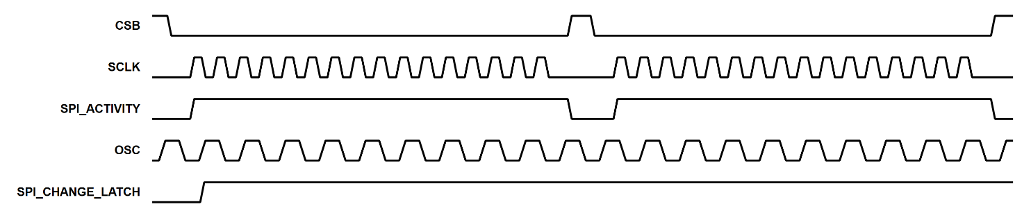 Figure 4. Detecting SPI Activity During MM CRC Calculation
Method 2: SPI Writes Outside of CRC Calculations
When the CRC state machine is not actively calculating a new value (or is in the idle state), it looks for SPI writes (not reads) from the last rising edge of SCLK to the next rising edge of SCLK. It is not necessary for CSB to be low at the next rising edge of SCLK (this is possible if the ADA4254 is sharing SPI lines with another part).
The signal that is active during this time is sampled with the internal oscillator clock. If this signal is sampled correctly, a flag is set internally to indicate that the MM has changed and a new “Golden” CRC value is calculated before the state machine is kicked off again.
 Figure 5. Detecting a SPI write while the State Machine is inactive
Changes to the Memory Map During the ROM CRC Calculation
SPI activity detection is not performed during the ROM CRC calculation.
Troubleshooting MM CRC Flags
These exceptional events, where an MM CRC error is flagged, may happen individually or collectively. If more than one occurs simultaneously, implement each applicable resolution.
Case 1
Gain reset is enabled (G_RST_DIS is set to “0”) and an overvoltage condition occurs in one or more of the input amplifiers that lasts more than 200 μs. The gain in the Gain_Mux register resets to 1/16 without the user writing to the part (the state machine won’t detect any activity). The “Golden” value won’t be recalculated, and the MM CRC error flag is tripped.
Case 1 Resolution
If Gain reset is enabled, monitor the Gain Reset error flag (G_RST) and the MM CRC error flag (MM_CRC_ERR). It is recommended to also enable Fault Interrupts and read back from the error registers immediately after an interrupt. If both G_RST and MM_CRC_ERR are tripped, the desired gain will need to be re-written to the registers and the error flags reset.
Case 2
When the time between SPI writes is much less than the period of the oscillator clock, it is less likely that the SPI Change signal for a write operation will be sampled and the MM CRC error flag may trip because no write operation has been detected.
Case 2 Resolution
The part is only required to sample one SPI Change signal in a string of write operations, and the slowest possible oscillator clock is 800 kHz (1.25 μs period). If commands to the ADA4254 must be be sent quickly, the user must ensure that the last write operation has a CSB high time of at least 1.5 μs to allow the change flag to be latched by the oscillator clock.
Case 3
All write activity occurs during the 19 oscillator clocks of the MM CRC calculation or the 32 oscillator clocks of the ROM CRC calculation where the part isn’t looking for SPI writes.
Case 3 Resolution
Disable the MM & ROM CRC error flags, wait at least 40 μs, then write to the part, with the last command enabling the MM & ROM CRC error flags. 40 μs is the maximum possible duration for the ROM CRC calculation (assuming the slowest possible oscillator clock). The worst-case scenario is the MM & ROM CRC error flags are not disabled due to a write operation occurring at the very beginning of a calculation. If this happens during a MM CRC, it is likely that activity will be detected, the state machine will go idle, then the part detects a write using Method 2.
However, if this happens during a ROM CRC calculation, there is no way to force the state machine to go idle, so adding in a delay of 40 μs guarantees that if the write operation to disable the MM CRC and ROM CRC error flags happens at the beginning of the calculation, the rest of the intended write operations will occur after the calculation, while the state machine is idle. Method 2 can be used to trigger a recalculation of the “Golden” CRC.
resources/ada4254-ref-manual.txt · Last modified: 23 Dec 2021 17:29 by Jordyn Ansari