


This version is outdated by a newer approved version. This version (16 Dec 2020 01:37) was approved by Mark Thoren.The Previously approved version (21 Jun 2020 21:58) is available.
This version (16 Dec 2020 01:37) was approved by Mark Thoren.The Previously approved version (21 Jun 2020 21:58) is available.This is an old revision of the document!
Table of Contents
Activity: Boost and Buck converter elements and open-loop operation
Objective:
The objective of this activity is to explore some of the basic circuit blocks typically used in buck and boost converters. We'll operate these blocks to the point where they are “bucking” a high voltage to a low voltage and “boosting” a low voltage to a high voltage, and examine the open-loop properties of these modes of operation. We will also discuss the difference between synchronous and non-synchronous circuits, and continuous conduction mode versus discontinuous conduction modes. We'll start out by controlling these circuits by directly controlling the duty cycle of the switches, and then introduce the idea of peak current control, in which the switch that “charges” the inductor is turned on by a clock signal, and turned off when the inductor current reaches a certain level. Subsequent exercises will actively control these circuits in order to produce an accurate, stable output voltage that is insensitive to changes in input and output conditions.
Materials
- ADALM2000 (M2K) Active Learning module OR:
- Two-channel oscilloscope with external trigger input
- Two digital multimeters OR:
- additional ADALM2000
- ADALM-SR1 Switching Regulator Active Learning Module
- User Guide: ADALM-SR1 hardware
- EVAL-CN0508-RPIZ power supply OR:
- 0-12V, 3A Adjustable benchtop power supply
- LTspice files for this exercise
- TEMPORARILY at Fork of analogdevicesinc/education_tools
Background
The Activity: Buck Converter Basics lab activity was a first look into the operation of a very simple (and not very high performance) buck converter. The exercise details the operation of the ideal buck converter shown in Figure 1.

Figure 1. Ideal Buck Converter
A simple expression for output voltage as a function of input voltage and the duty cycle, is then derived:
This is followed by circuit construction, measurements of the open-loop properties of the circuit, and finally, “closing the loop” so that the output voltage remains constant, at the desired voltage, regardless of changes in loading.
This exercise will expand on those concepts, deriving a converter that “boosts” a low voltage to a high voltage. We will also design a more practical open-loop buck converter, and introduce a circuit that controls peak inductor current, rather than duty cycle. Subsequent exercises will close the loop around these circuits and examine loop stability and time-domain response. An appendix covers practical aspects of switching converter design such as current sensing, timing generation, selection of MOSFETs and diodes, and gate drive circuitry.
Activity 1: An Ideal* Open-Loop Boost Converter Simulation
* (This exercise will use the term “ideal” extensively. A more accurate term would be “almost ideal” - LTspice requires finite numbers in certain locations - switch on and off resistances can't be zero or infinity, so we're using values small enough and large enough to have negligible impact on the results.)
Open the OL_Boost_concept_ideal_sw.asc LTSpice file. Notice the differences between this circuit and the buck converter:
- One side of the inductor is connected directly to the input supply.
- The switches are rearranged, with S1 allowing the input supply to be connected directly across the inductor, and S2 allowing the inductor to be connected or disconnected from the output.
As with the buck basics lab, let's keep two things in mind at all times:
- Current through an inductor can't change instantaneously
- The DC voltage across an inductor is zero
The figure below shows the “charge” state of the circuit’s operation, where S1 is closed and S2 is open.

Figure 2. Boost Converter Charge
When S1 closes, the left-hand side of the inductor is connected to the 5V supply, and the right-hand side is connected to ground. This means the voltage across the inductor is simply the 5V supply. This “charges” the inductor with a current that ramps up with a positive slope of:
Note: The polarity of the voltage across the inductor is arbitrary, we're using the convention that a positive voltage is one that causes an increase in energy stored in the inductor.
The next figure shows the other state, with S1 open and S2 closed.
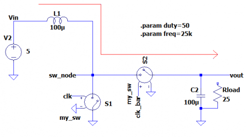
Figure 3. Boost Converter Discharge
When S2 closes, the left-hand side of inductor L1 is still connected to Vin, while the right-hand side is now connected to Vout. The current through L1 is now flowing to the output, and decreasing with a negative slope of:
Similar to the buck converter basics activity 1 the “freq” and “duty” parameters set the frequency of the switching to 25kHz and the duty cycle of the voltages imposed on this switch node (sw_node) to 50%. That is, the righthand side of the inductor spends half of the time connected to ground (charging phase), and half of the time connected to the output (discharging phase). Run the simulation, and probe sw_node, Vout, and the current through inductor L1. Zoom in toward the end of the run after the startup transient damps out (after 8ms). (You can right-click, Auto range y-axis to line up the two waveforms.)
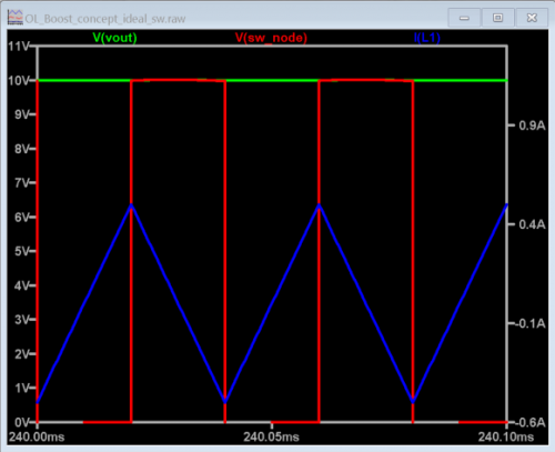
Figure 4. Boost Converter Switch Node, inductor current, and Output
Observe the peak and valley of the waveform I(L1) (green waveform), noting the current ripple. Using the cursors from peak to peak, we can observe that the inductor is charging and discharging linearly (with the period of 1/25kHz, or 40us, with a duty cycle of 50% making ts1 and ts2 20us each).
The output voltage is almost exactly 10V - double the input voltage - with a small ripple imposed. Verify that the previously solved equations are true, using the cursors to measure the inductor current waveforms.
For the “charge” phase:
And for the “discharge” phase:
Revisiting the concept of zero DC across an inductor, how can we find the output voltage of a boost converter knowing the input voltage, frequency, and duty cycle? “Zero DC across an inductor” means that over a long period of time, the average volt-second product is zero. Thus:
Where tS1 is the time that S1 is closed, tS2 is the time that S2 is closed. Rearranging, we see that:
Note that
is the duty cycle of the switch node, we can rewrite the expression for VOUT as a function of duty cycle:
Since our duty cycle is based off ts1 and ts2, and the duty cycle is always between 0% and 100%, the above equation demonstrates that the average output voltage is always equal or larger than the input voltage, a basic property of a boost converter, and at a 50% duty cycle, the output voltage is double the input voltage.
Now change the duty cycle in the simulation and re-run. The following are screenshots show the output voltage at 20% duty cycle(expected output of 6.25V) and 80% duty cycle(expected output of 25V).

Figure 5. Boost converter output with a duty cycle of 20%

Figure 6. Boost converter output with a duty cycle of 80%
Can you boost to an arbitrarily high voltage? See Appendix: “Extreme Boosting” to find out.
Load Regulation
So far we've operated the boost circuit unloaded. In this condition, the duty cycle to boost factor relationships held true, but what happens if you start to draw current from the output (as you would in a practical circuit - after all, a power supply exists to power stuff!) Furthermore, consider the boost converter's output switch (S2). If we look at the current waveform and the voltage waveform of the unloaded circuit, we see that for part of the cycle, the inductor current goes negative, and when this occurs, the output voltage is ramping DOWN! This seems counterproductive for a boost converter, doesn't it? This mode of operation has a name - “Forced Continuous Conduction Mode”. It is forced because the switches always impose a voltage across the inductor, so its current is always either ramping up or down.
Next, connect the 25 ohm load resistor to the output node (drawing an average current of 0.4 amps from the 10V output). Note that the impact on the output voltage is minimal, and the inductor current is still ramping up and down with the same peak-to-peak ripple, however the current is now always positive (flowing from input to output, according to our convention.)

Figure 7. Ideal Boost Converter with 25Ω load
But are we still FORCING this circuit to conduct continuously? We'll find out shortly…
Activity 2: A real Open-Loop Boost Converter
Open OL_Boost_concept_actual.asc in LTspice (see Figure 8). This simulation is a close approximation of the ADALM-SR1 configured for this mode.

Figure 8. Open-Loop Boost LTspice Schematic
Note that the simulation includes some of the non-ideal aspects of the real-world circuit:
- Replace the ideal diode with a real diode, a MBRS340 (which is a close variant of the MBRA340 on the SR1)
- Add the series resistance of three windings of the Wurth '141 inductor.
- Replace the switch with an IRF7468 (close to the IRF7470 on the SR1)
- Add the 0.1Ω current sense resistors
- Add output capacitors, with ESR
Note that this schematic still contains many simplifications - the gate driver is not shown, nor are the current sense amplifiers. And since the circuit is powered from an ideal voltage source (zero impedance), input capacitors can be eliminated. This will be a recurring theme, deciding what to simulate and what to assume is close enough to ideal that it can be eliminated from the simulation in the interest of speed, or in some cases, converging at all. The most obvious substitution is the replacement of the top switch with a diode. This will be discussed in more detail shortly, but for now, note that a diode is in fact a switch that conducts when the voltage at the anode is higher than the voltage at the cathode, and does not conduct when the polarity of the voltages are reversed.
BEFORE APPLYING POWER… Configure the ADALM-SR1 board as shown in Figure 9 below:
- Duty Cycle: Manual
- Mode: Duty Cycle
- FET Sel: Boost
- Current Sense: High
- Current Threshold: Manual
- Inductance: 4 Taps
- Load Resistors: enable 2×200Ω, 100Ω, 50Ω (25Ω total)
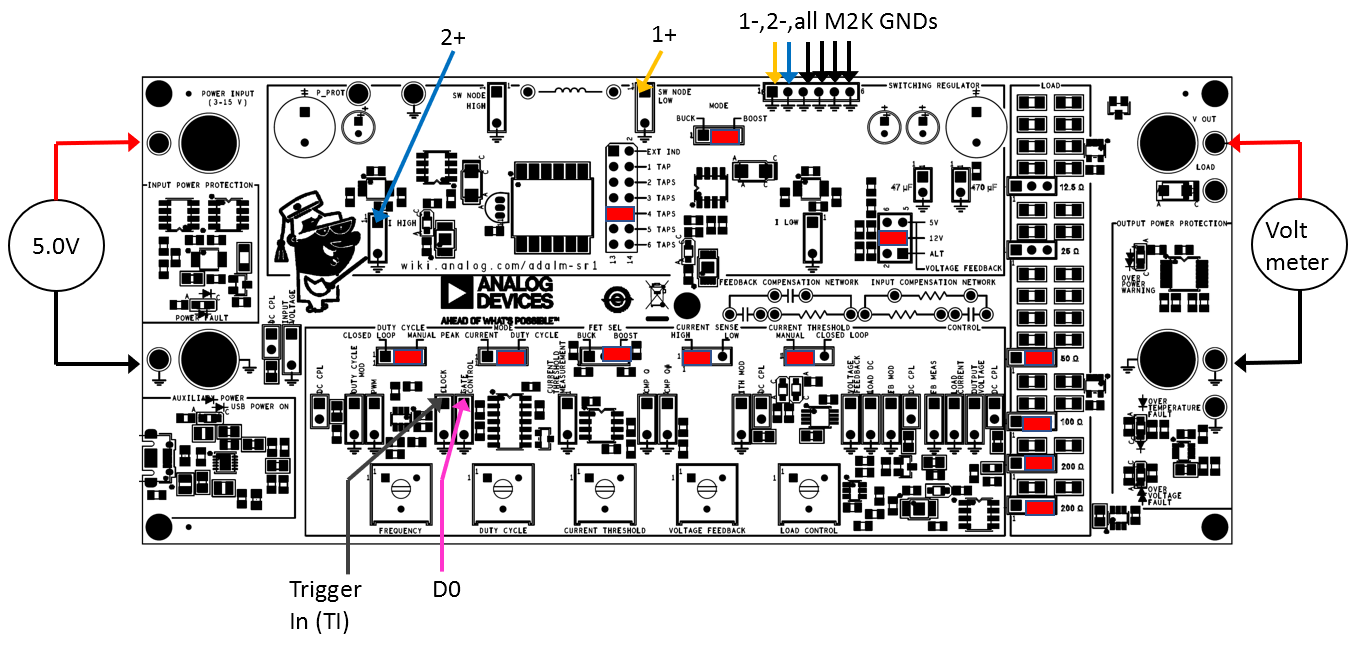
Figure 9. ADALM-SR1 configuration for Open-Loop Boost, Duty Cycle Control
Set potentiometers to the following approximate settings:
Frequency: 3:00 Duty Cycle: 9:00 Minimum On Time: 7:00 (fully counterclocwise) Current Threshold: 3:00 Voltage Feedback: 12:00
Set potentiometers to the following approximate settings:
- Frequency: 3:00
- Duty Cycle: 9:00
- Minimum On Time: 7:00 (fully counterclocwise)
- Current Threshold: 3:00
- Voltage Feedback: 12:00
Connect a 5V, 1A USB power supply to the Auxiliary Power micro USB jack. At this point, the frequency and duty cycle can be fine-tuned by looking at the D0 signal in Scopy's logic analyzer. Set the frequency to 20kHz (50μs period) and duty cycle to 25% (high time of 12.5μs)
Add Logic Analyzer Plot
Ramp the Power Input to 5V and observe the current sense and switch node waveforms. Note that Scopy's vertical scale can be entered arbitrarily - enter a value of 350mV/Div, which corresponds to 500mA/Div. Figures 10 and 11 show simulated vs. measured results, respectively, at 25% duty cycle. Note that the output voltages match quite well, both are very close to 6V. This is less than the predicted 6.66V of an ideal boost converter, however, note that this circuit starts off with about a 0.4V drop due to to the output diode. Output current is about 240mA (6V/25Ω), which will cause another 275mV drop due to the two 0.1Ω sense resistors and the 0.95Ω resistance of the inductor. This is a total drop of about 0.676V, almost exactly the difference between the ideal case and reality!

Figure 10. Open-Loop Boost Simulation, 20kHz, 25% Duty Cycle, 25Ω Load
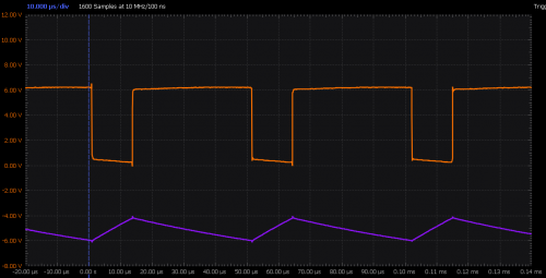
Figure 11. Open-Loop Boost Operation, 20kHz, 25% Duty Cycle, 25Ω Load
Next, increase the duty cycle to 50%. Figures 12 and 13 show simulated vs. measured results, respectively, at 50% duty cycle.

Figure 12. Open-Loop Boost Simulation, 20kHz, 50% Duty Cycle, 25Ω Load
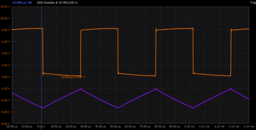
Figure 13. Open-Loop Boost Operation, 20kHz, 50% Duty Cycle, 25Ω Load
Going Further
Try experimenting with the various load resistors and duty cycle potentiometer. The ADALM-SR1 does have a level of protection from stressful operating conditions: load and inductor overheating, output overvoltage, etc., but in this configuration please observe the following precautions:
- Keep duty cycle under 50%
- Keep the input voltage at or below 5V
- Leave the frequency at 20kHz
Activity 3: Synchronous vs. Non-Synchronous Circuits
Describe in more detail why we replaced the top switch with a diode, simulation with an ideal diode, and show that it's equivalent to the synchronous circuit when operating in CCM.
Activity 4: Discontinuous Conduction Mode
With the circuit still configured as in Activity 2, reduce, or “lighten”, the output load by removing the 50Ω and 100Ω load resistor jumpers, leaving the two 200Ω jumpers in place for a total load resistance of 100Ω. You should notice the switch node and inductor current take on a drastically different shape. Figure X shows the switch node and inductor current at a 25% duty cycle. The output voltage jumps to 7.74V, HIGHER than the 6.67V predicted by the output voltage equation above (even with the drop of the boost diode and the IxR drop of the sense resistors and inductors.)
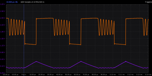
Figure x. DCM, 20kHz, 50% Duty Cycle, 100Ω Load
Figure X shows the switch node and inductor current at a 50% duty cycle. The output voltage is measured at 11.6V, again, higher than predicted.

Figure x. DCM, 20kHz, 50% Duty Cycle, 100Ω Load
This is a second mode of operation called “Discontinuous Conduction Mode”, and clearly it needs some additional equations to describe the relationship between input voltage, duty cycle, and now, output loading…
Activity 5: An Open-Loop Buck Converter
(Simulation and ADALM-SR1, no need to separate, buck basics lab handles the ideal case.)
Activity 6: Peak Current Control
Controlling a switch's duty cycle in order to adjust the output voltage of a switching regulator seems like a straightforward method, and we'll set up the circuit to automatically adjust the duty cycle to maintain a constant output voltage in the next exercises. But it turns out that there are advantages to not directly controlling the duty cycle, but rather, to control the maximum, or peak, inductor current at each and every clock cycle. This mode of operation (“current mode”) has dynamic advantages in closed-loop operation that will be explained in the next exercise. But since this exercise is focusing on open-loop operation, we'll just describe and demonstrate the circuits operation, and point out one very important advantage of peak current control - the overall circuit is inherently short-circuit proof!
Open OL_boost_peak_current_control.asc, shown in Figure X.
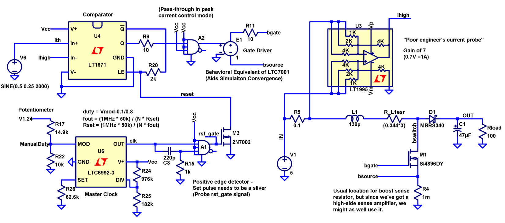
Figure X. Peak Current Control Circuit, Boost Mode
The implemenation of the ADALM-SR1 peak current control circuit differs from that of a typical boost converter, such as the LT1930 shown in Figure X, however the end result is similar.

Figure X. LT1930 Boost Converter Block Diagram
In both circuits, a master oscillator sets the operating frequency. The rising edge of the clock is shaped into a narrow “set” pulse (or “sliver”). A narrow pulse is necessary as it sets the “minimum on-time” of the switch, and hence, the minimum boost factor. So in theory, the output of an unloaded asynchronous boost converter would rise without bound! In practice, there is always some limiting factor, shuch as the feedback resistance, parasitic capacitances, or other losses that limti the upper bound. Furthermore, converters designed to operate at very light loads will incorporate additional methods - such as blanking the clock entirely.
Assume that both the LT1930 and ADALM-SR1 start out with zero inductor current (right after applicaiton of power), and the current control signal (usually called ITH) is nonzero. Also assume the LT1930's R-S flip-flop is reset, and the ADALM-SR1's LT1671 comparator's Q output is low, Q# is high, such that the LT1671 is latched OFF, even though its IN+ input (ITH) is higher than its IN- input (Ihigh current sense signal).
When the set pulse occurs, the LT1930's R-S flip flop is… set, the output switch is turned on, and inductor current starts to ramp up. Similarly, the ADALM-SR1's set pulse momentarily pulls the LT1671's LE pin low, unlatching the comaprator, which in turn turns on the switch (M1), and inductor current starts to ramp up.
Both the LT1930 and ADALM-SR1 current signals also begin to ramp up as inductor current increases. When the current sense signal reaches the same voltage as ITH, the comparators trip, shutting off the respective switches, and the process begins again at the next set pulse.
That is quite a lot of text to describe a rather strange (for those who've never seen it before), so the best thing to do is start out running the LTspice simulation, which is configured to modulate ITH with a 2kHz sinusoid. Results are shown in Figure X. Note that we can “trick” LTspice into displaying the ITH and Ihigh signals as the current they represent by adding some arithmetic to the traces - right-click the label (V(ith), for example), then add “ *(1A/0.7V) ”, which is the gain of the current sense circuit.

Figure X. Peak Current Control Waveforms
Next, configure the ADALM-SR1 for open-loop boost, peak current control as shown in Figure X.

Figure X. ADALM-SR1 configuration for Open-Loop Buck, Peak Current Control
There is indeed provision on the ADALM-SR1 to modulate the ITH signal exactly as shown in the simulation, and that technique will be used in a future exercise to characterize the frequency response of the circuit. In this exercise, we'll just focus on steady-state behavior. Set the clock frequency to 20kHz, duty cycle to 50% (midscale, can be approximate). Set channel 2 vertical scale to 340mV/division, corresponiding to 500mA per division. Set the current threshold potentiometer such that the current peaks are at about to about 1.5 divisions (750mA). In this configuration, vary the input voltage from 5V to 10V, and vary the output load from 50Ω to 100Ω. These conditions are shown in Figure X. Note the changes in rising slope (which will be steeper with higher input voltage), falling slope (which will be shallower when the output voltage is higher), and that the circuit transitions between continuous and discontinuous modes. But in all cases, the peak current stays fixed.

Figure X. Switch Node and Inductor Current, Various Conditions
(Click to open in same window if animation doesn't play)
Conclusion
This lab exercise detailed the “power path” for non-synchronous boost and buck converters, illustrating duty-cycle control and peak current control. These circuits would be practical by themselves in a well-controlled environment, where input voltage and output loading conditions are well-known and stable. But real-world applications rarely fall into this category, so it is necessary to add a means of sensing the output voltage and adjusting the operating parameters (duty cycle or peak current) to maintain regulation as conditions change. This will be covered in the next exercises.
Appendix: Extreme Boosting
Simulations at 99% duty cycle, and why high boost factors are almost never practical in real life.
Appendix: Current Sense Techniques
There are several methods of measuring current in a circuit. Like any electrical measurement, the act of measuring the current will have some effect on the circuit's operation. One of the least obtrusive when a convenient measuring point is physically accessible is a current probe. A wideband current probe that sensitive to DC (a steady-state current) uses a combination of a current transformer that is sensitive at high frequencies and a Hall-effect sensor that is sensitive to DC. Fine tuning the frequency responses of these curcuits such that the combined response is “flat” over all frequencies is a delicate task, and is one reason current probes tend to be very expensive. Also, current probes require that the curent flow through the probe's head, so an extra wire may need to be introduced into the circuit. If the added inductance of the extra wire is significant compared to other inductances in the cirucit, then circuit operation may be significantly impacted. Figure X shows a current probe being used to measure the ADALM-SR1 inductor current. The inductance selection jumper is replaced with a short jumper wire that is looped through the current probe twice to double the sensitivity (twice the current effectively flows through the probe.)

Figure x. Probing ADALM-SR1 Inductor Current W/ Tektronix P6042 Probe
But of course chip manufacturers can't ship a current probe with every device, so other smaller, lower cost, and lower (but adequate) performance methods must be used. Some of these include:
* Sensing the voltage across an external sense resistor, with an amplifier that is optimized for the common-mode voltage range (accurate, but lossy) * Sensing the voltage across the RDS(on) of the switching MOSFET (not accurate, but not lossy) * Sensing the voltage across the inductor's ESR (not accurate, not lossy, but requires filtering)
While some of these methods are not very accurate in absolute terms, this is typically not a concern as the current measurement (and current control) is enclosed in an outer voltage control loop that IS accurate. Also, these methods do not always measure the entire current waveform; depending on the sense amplifier topology and position within the circuit, they may only “catch” the rising slope of the current waveform, and they may not be able to sense reverse currents (even if they are small, as during the “ringing” portion of a discontinuous switch node waveform“. This is fine if that is what is important (as it is in an actual switchign regulator), but for a complete analysis, a complete picture of both rising and falling waveforms, including negative currents.
The ADALM-SR1 includes two sense resistors and two LT1995, 30MHz difference amplifiers in a differential gain of 7. This provides a simple, high-bandiwdth, DC-coupled picture of inductor current. While either amplifier could be used for either boost or buck operation, the “high side” amplifier is used for boost topology, and the “low side” amplifier is used for the buck topology. In both of these cases, the amplifier is at the “non-switching” side of the inductor such that its common-mode voltage is costant, and the complete inductor waveform is visible.
LT1995 simple situations
Appendix: Gate Divers
The MOSFETs in the LTspice simulations in this exercise are all either directly driven from a pulse voltage source, or by a VCVS (voltage-controlled voltage source) that “level shifts” a ground-referred signal. But what is used in the actual ADALM-SR1 circuit, and why aren't we using its LTspice model?
Driving the gate of the low-side (boost) MOSFET seems like such a simple job - Ground the gate, and the MOSFET is off. If you measure the resistance from the gate to ground, the resistance is so high that it is likely that your meter will overrange (assuming the board is clean from flux or other contamination.) And the low threshold voltage of the IRF7470 makes it compatible with 5V logic-level signals. But there are subtleties to driving a MOSFET: Even the boost MOSFET can be tricky to drive - as the MOSFET is turning on, the gate-drain capacitance will draw significant current. And if for some reason the gate drive voltage is too low, due to a collapsing housekeeping supply for example, the MOSFET may not be driven fully on, resulting in excessive power dissipation.
The high side (buck) MOSFET is much trickier - the ground-referred gate control signal needs to be “level-shifted” and referred to the MOSFET's source, which toggles back and forth between about -0.4V and the input voltage - quite a challenge. For these reasons, LTC7001s were used. The LTC7001 is specifically designed to drive N-channel MOSFETS, addressing all of these issues.
Figure X shows LTspice simulations of both the LTC7001 gate driver, as well as its VCVS “equivalent”.
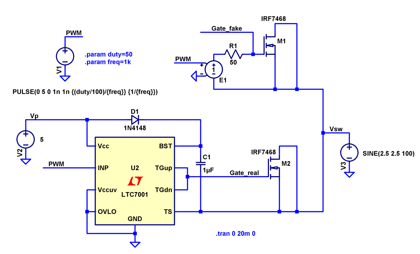
Figure X. LTC7001 vs. VCVS Gate Drivers
An important aspect of the LTC7001 is that it has an internal charge pump that will keep the BST capacitor charged even if the cirucit isn't switching. This allows the ADALM-SR1 to function at arbitrarily low frequencies, even zero. In fact, the top MOSFET, which is the switching element in buck configurations, is held continuously ON when the board is configured as a boost converter. Other gate drivers may REQUIRE that the source pin be periodically driven to ground, as would occur in normal buck converter operation.
With that in mind, run the OL_gate_drivers.asc simulation, the results of which are shown in Figure X.

Figure X. LTC7001 vs. VCVS Gate Drivers
Note that in both cases, the gate drive signal is a nice, “strong” or “sharp” square wave imposed between the MOSFET's source and gate.
Appendix: Timing Generation
Timing on the Switching Regulator Active Learning Module is generated by an LTC6992-3 pulse-width modulator and variable frequency oscillator. The frequency range is XX to YY, and the PWM duty cycle of the -3 variant extends from zero to 95%, never reaching 100%. This is a great device for generating timing signals for this board because it can be used both as pulse-width modulator and a clock. As a PWM generator, a simple 0-1V control signal to set the duty-cycle to 0-100% (clipped at 95% for the -3). To use the devices as a clock generator, simply set the duty cycle to 50% by setting the MOD pin to 0.5V.
The -3 variant is used for two reasons: First, it limits the maximum boost factor, providing some redundancy to the overvoltage shutdown circuits. Second, the peak-current control circuit is still active in direct-duty-cycle control mode. This circuit requires clock edges in order to reset, and limiting the duty cycle to 95% ensures that edges occur. (A duty cycle of 100% is a signal that is always high, so there are no edges to reset the current limit.)
Another point about the LTC6992 - the “classic” method of generating a PWM signal is to compare a sawtooth or triangular reference ramp to the modulation signal as shown in the circuit below:
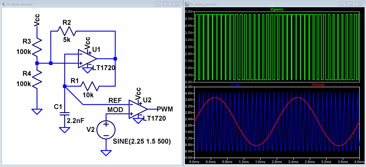
Where V2 is the modulation signal. The upper trace shows the PWM output; note that the duty cycle is high when the modulation signal is high, and vice-versa. The LTC6992 is functionally very similar, with the exception that the response is not immediate - the modulation bandwidth is approximately 10kHz, roughly equivalent to placing a 10kHz, 1-pole filter at the output of V2 in the figure above. As long as the loop bandwidth of the switching regulator is significantly lower than 10kHz (a safe assumption in most of our use cases), the impact is minimal.
Appendix: "Engineer Proofing"
Given the fact that bad things sometimes happen to good people, and even the best engineers make mistakes, The ADALM-SR1 includes numerous protection features:
* Input Overvoltage (to +40V) * Input Undervoltage (between 0V and 3.3V) * Input Reverse Voltage (to -40V) * Inductor overheating (above 50C) * Load resistor overheating (above 50C) * Output Overvoltage (above 22V)
These are described in comments in the OL_engineer_proofing.asc schematic. Students are strongly encouraged to open and run this simulation, as it represents some “real world” design decisions that were wrapped around an otherwise “purely instructional” circuit.
Slide Deck
A slide deck is provided as a companion to this exercise, and can be used to help in presenting this material in classroom, lab setting, or in hands-on workshops.
(Insert slide deck here)
Return to Lab Activity Table of Contents
university/labs/open_loop_boost_and_buck_adalm2000.1608078780.txt.gz · Last modified: 16 Dec 2020 01:33 by Mark Thoren