


This version is outdated by a newer approved version. This version (23 Mar 2020 19:35) was approved by Mark Thoren.The Previously approved version (11 Mar 2020 18:10) is available.
This version (23 Mar 2020 19:35) was approved by Mark Thoren.The Previously approved version (11 Mar 2020 18:10) is available.This is an old revision of the document!
Table of Contents
Activity: Buck Converters: closed loop operation
Objective:
The objective of this activity is to close the loop around the buck converter developed in the previous exercise such that the output voltage remains constant as the input voltage and output loading conditions vary. First, the loop will be closed in an “overcompensated” manner, such that the DC output voltage is correct, disregarding stability, transient response, and other AC parameters. The power stage AC response will then be characterized, essential in developing a robust and stable control loop. The loop will then be closed using the “obvious” method of voltage-mode control, that is, adjusting the duty cycle directly in response to an error in output voltage. Next, a current control loop will be introduced, and the advantages and disadvantages of this method explored.
Several analysis methods will be demonstrated using LTspice - AC simulation of continuous time circuits, extracting the frequency response of switching circuits using step and measure techniques in LTspice, Middlebrook's method for extracting open loop gain from a closed loop system. Where possible, these will be replicated on the ADALM-SR1 hardware.
Materials
- ADALM2000 (M2K) Active Learning module OR:
- Two-channel oscilloscope with external trigger input
- Two digital multimeters OR:
- additional ADALM2000
- ADALM-SR1 Switching Regulator Active Learning Module
- User Guide: ADALM-SR1 hardware
- CN0508-RPIZ power supply OR:
- 0-12V, 3A Adjustable benchtop power supply
Background
Applying traditional control theory to switching regulators presents some challenges. A continuous time system - even a “messy” one that may be nonlinear or time-variant - can often be approximated by a linear system by limiting the range of amplitudes and / or frequencies. There is no such good fortune with switching regulators - the power stage inherently involves a switching circuit that traverses several distinct states. One approach to this problem is to derive a continuous time model that approximates the behavior of the power stage at the timescales of interest. Once this model is derived, traditional methods can be used to design feedback compensators to meet the application requirements. Application Note 149: Modeling and Loop Compensation Design of
Switching Mode Power Supplies is an excellent resource for this general approach, while this lab exercise will focus on the specific case of the ADALM-SR1. Some additional resources on the subject are:
Loop Gain and its Effect on Analog Control Systems
Application Note 170: Honing the Adjustable Compensation Feature of Power System Management Controllers
Application Note 140 Basic Concepts of Linear Regulator and Switching Mode Power Supplies
Activity 1: An Overcompensated Voltage-Mode Buck Converter
Before we dig into too much theory, let's at least get the buck converter into regulation… The goal of this experiment is to produce an accurate output voltage, regardless of changes in input voltage (“line regulation”) and changes in output loading conditions (“load regulation”). We'll do this by dynamically changing the duty cycle of the PWM generator in response to changes in the output voltage - if the output voltage is a bit too high, reduce the PWM duty cycle. If the output voltage is a bit too low, increase the PWM duty cycle.
This is called “voltage mode” control because the error signal (how far we are off from the desired output voltage) directly controls the input voltage to output voltage ratio (set by the duty cycle.)
Figure X below shows the buck power stage from the open-loop exercise, but with the duty cycle potentiometer replaced by an op-amp circuit configured as an inverting integrator. This circuit compares a scaled version of the output voltage against an accurate 1.25V reference voltage, and performes the following actions, stated qualitiatively:
- If the output voltage is a little bit too low, the output voltage ramps up slowly.
- If the output voltage is MUCH too low, the output voltage ramps up quickly.
- If the output voltage is a little bit too high, the output voltage ramps down slowly.
- If the output voltage is MUCH too high, the output voltage ramps down quickly.
- And finally, if the output voltage is “just right”, hold the output voltage constant

Figure 1. Voltage Mode Buck Converter
But since the integrator output is connected to the LTC6992-1's MOD pin, an increase / decrease in voltage will directly cause a corresponding increase / decrease in the MOSFET's duty cycle, which will tend to bring the output voltage toward the “just right” voltage.
Also note the following simplifications:
- LTC7001 gate driver replaced with a voltage-controlled voltage source with a gain of 1
- MOD positive clamp circuit replaced with an ideal diode and voltage source
Open the CL_buck_voltage_mode.asc simulaton and run it. Observe the turn-on transient, which has quite a bit of overshoot, but then stabilizes at 5.0V. Zoom in on the switch node and inductor current after the intial transient, shown in Figure X. Note that the circuit is operating in DCM.

Figure 2. Voltage Mode Buck Converter Simulatoin, switch node and inductor current
BEFORE APPLYING POWER… Configure the ADALM-SR1 board as shown in Figure X below:

Figure 3. ADALM-SR1 Configuration for Voltage Mode Buck Operation
Install the following jumpers:
- Duty Cycle: CLOSED LOOP
- Mode: Duty Cycle
- FET Sel: BUCK
- Current Sense: LOW
- Current Threshold: MANUAL
- Inductance: 4 Taps
- Load Resistors: enable 2×200Ω, 100Ω, 50Ω, 25Ω (12.5Ω total)
Set potentiometers to the following approximate settings:
- Frequency: 3:00
- Duty Cycle: 12:00
- Minimum On Time: 7:00 (fully counterclocwise)
- Current Threshold: 3:00
- Voltage Feedback: 5:00 (fully clockwise)
Additionally - install the following components:
- 0.1μF capacitor between TP22, TP24
- 10kΩ resistor between TP21, TP19
- 10kΩ resistor between TP14, TP17
Connect a 5V, 1A USB power supply to the Auxiliary Power micro USB jack. At this point, the frequency can be fine-tuned by looking at the D0 signal in Scopy's logic analyzer. Set the frequency to 20kHz (50μs period)
Ramp the Power Input to 12V and observe the current sense and switch node waveforms. Note that Scopy's vertical scale can be entered arbitrarily - enter a value of 350mV/Div, which corresponds to 500mA/Div. Figure X shows the measured results; compare with the simulated result in Figure X.
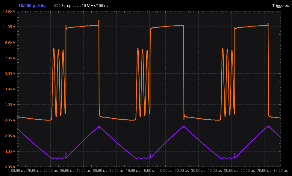
Figure 4. Measured Results, switch node and inductor current
Decrease the input voltage to 8V and note the following: Duty cycle increases automatically to maintain 5V at the output The mode of operation changes from DCM to CCM.
Activity 2: Closed-loop, current-mode, overcompensated for guaranteed stability
The goal of this experiment is identical to the previous one: to produce an accurate output voltage, regardless of changes in input voltage or output loading. But instead of directly changing the duty cycle of the PWM generator, we'll instead modulate the peak inductor current - if the output voltage is a bit too high, reduce the peak inductor current. If the output voltage is a bit too low, increase the peak inductor current.
This is called “current mode” control because of the error signal (how far we are off from the desired output voltage) is directly compared to the peak inductor controlling the current in the circuit. Conceptually this makes the inductor a controlled current source.
Consider Reordering, put after Voltage Mode is done.
Activity 3: Voltage-mode loop optimization
The previous examples were overcompensated so that the steady-state operation of the control loop could be analyzed, without too much concern that it would burst into oscillation. The next few experiments will demonstrate the drawback of overcompensation (slow response to changes in conditions), and outline the procedure for making it a bit more “snappy”, while still not oscillating.
The first step in speeding up the response by adjusting the compensator is to understand the response of the power stage to the output of the compensator. Or stated another way, to find the transfer function from a wiggle at the power stage's control input to the output actually moving. A great reference for some of these ideas is Linear Technology (Analog Devices) Application Note 47, Appendix C “The Oscillation Problem - Frequency Compensation Without Tears” (insert URL)
Buck Power Stage Continuous model, voltage-mode
Consider the ADALM-SR1 power stage when configured for open-loop, duty cycle control mode, with the LTC6992-3 PWM generator providing the gate control:

Figure 5. Buck Switching Power Stage
The property of this circuit that needs to be extracted is the transfer function from a “wiggle” at the MOD pin to a “wiggle” at the output (labeled “a”). Intuitively, sweeping the voltage at the MOD pin from 0V to 1.0V will produce a 0 to 100% duty cycle at its OUT pin. The power stage will then translate this duty cycle to an output voltage of 0V to 12V, on the condition that the circuit is operating in CCM. Following the logic in AN149, this circuit SHOULD be roughly equivalent to the following, purely linear circuit:

Figure 6. Buck Linearized Power Stage
noting that the inductance, output capacitors, and load resistor are identical to the switched circuit. E1 is a voltage-controlled voltage source, representing the inherent gain of 12 in the switching circuit. This circuit may look familiar - it is an RLC lowpass filter, so we should be able to simulate it as such with a .AC analysis. Including this SPICE directive:
.ac dec 25 5 50k
will allow us to measure the transfer function from 5Hz to 50kHz, with the result shown here:

Figure 7. Buck Linearized Power Stage Response, AC Analysis
Which is great! But… remember that we can't use a .AC directive on the switching circuit because it has no operating point around which it can be analyzed. What we can do is apply a stepped frequency / measure analysis, described in the link below. Replacing the .AC directive with the following:
.meas Aavg avg V(a)
.meas Bavg avg V(b)
.meas Are avg (V(a)-Aavg)*cos(360*time*Freq)
.meas Aim avg -(V(a)-Aavg)*sin(360*time*Freq)
.meas Bre avg (V(b)-Bavg)*cos(360*time*Freq)
.meas Bim avg -(V(b)-Bavg)*sin(360*time*Freq)
.meas GainMag param 20*log10(hypot(Are,Aim)/hypot(Bre,Bim))
.meas GainPhi param mod(atan2(Aim,Are)-atan2(Bim,Bre)+180,360)-180
.param t0=0.01m
.tran 0 {t0+25/freq} {t0}
.step dec param freq 5 50K 5
.save V(a) V(b)
.option plotwinsize=0 numdgt=15
performs a roughly equivalent analysis, stepping the input frequency from 100Hz to 100kHz, but at each step, capturing the input and output waveforms and performing a Fourier analysis to extract gain and phase. The result is shown below:

Figure 8. Buck Linearized Power Stage Response, Stepped Analysis
So now that we're convinced that these two simulation methods produce approximately the same result (Note: dig into discrepancies that do exist!), we can apply the second method to the switching circuit, with the following result:

Figure 9. Buck Switching Power Stage Response
At low frequencies, it is remarkably similar! Note the strange behavior around 10kHz - this is because the power stage is switching at 20kHz, so it only has 20,000 discrete “opportunities” to modify the output voltage per second, and thus can be looked at as a sampled system - and all sampled systems are subject to Nyquist criterion, and will alias if this is violated. (We can dig into that later…)
But we found the dominant pole of the power stage - about 362Hz for the linearized model, and about 103Hz for the switching model!
Dig into discrepency - are we discontinuous?
The last step, naturally is to measure the actual power stage and see how it compares to simulation. Configure the ADALM-SR1 as shown in Figure 10 below.
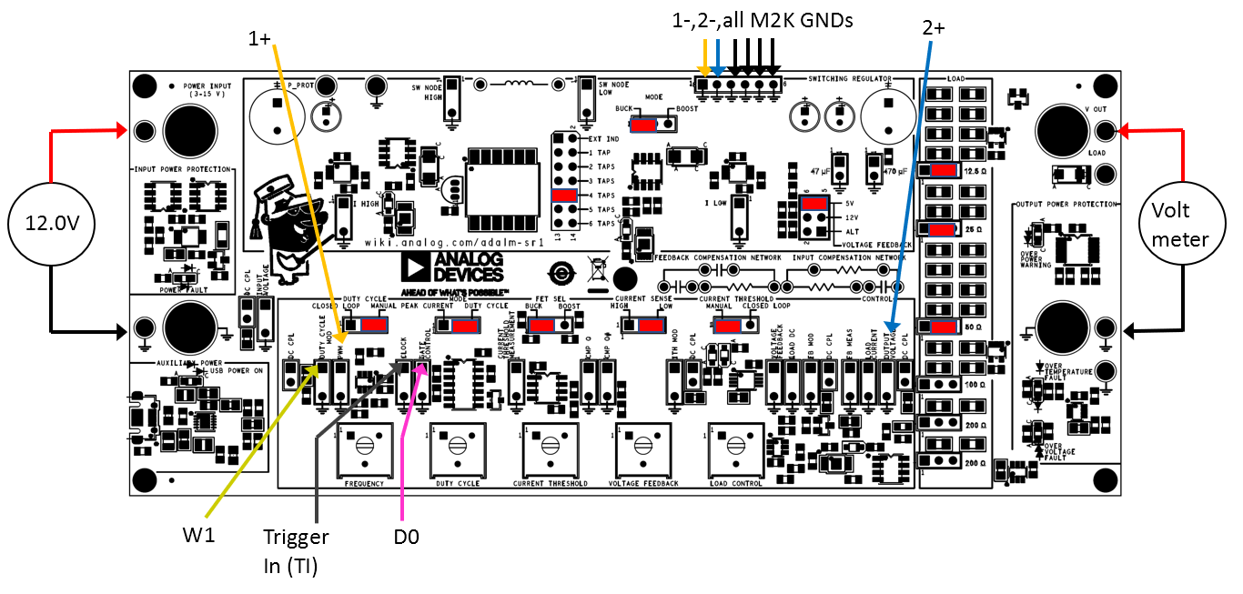
Figure 10. ADALM-SR1 Config. for Voltage Mode Buck Power Stage Response
This is also the point in our experiment where things get “interesting”, in the sense that real-world messiness (switching noise) needs to be carefully balanced with signal levels and measurement resolution: No matter how big you make the inductance and output capacitor, there will always be some switching residue that will obscure the signal you're trying to measure.
- Applying a large stimulus to the power stage will result in a larger signal that will be easier to measure, however, the response may become nonlinear (distort).
- Applying a small signal will tend to keep the response more linear, but the smaller output signal will be more difficult to disginguish from noise.
Start by connecting the ADALM-SR1's auxilary power. Set the input voltage to 12V. In Scopy's Logic Analyzer, verify that the switching frequency is still set to 20kHz. Set the duty cycle such that the output voltage is 5V. At this point the switching circuit is in the same conditions it would be if the loop were still closed, that is, the error integrater would adjust the duty cycle to the same value as we just did. The difference is, IF something did change: if the load were increased or the input voltage dropped, output would drop momentarily, but the error integrator would bring the output back into regulation by increasing the duty cycle. (The opposite would happen if the load were decreased or the input voltage increased - the error integrator would reduce the duty cycle.)
To determine the frequency response of the power stage around this operating point, we need to sinusoidally stimulate (“wiggle”) the duty cycle around, and see how the output responds. Intuitively, if you wiggle the MOD pin slowly, the delay through the LTC6992-3 will be negligible, and the delay due to the L-C filtering effect of the inductor and output capacitors will also be negligible. But as you continue to increas the frequency of the stimulus, there will be a measurable phase lag at the output, and the amplitude of the output “wiggle” will be smaller than it was at lower frequencies.
Ideally, we would do a complete frequency response and try to replicate the full Bode plot from the LTspice simulation, and Scopy does have a network analyzer feature that would do this very nicely for the linearized circuit. However, the noise that is present on our measured signal has the potential to confuse the network analyzer. But we can make some simplifying assumptions and measure the -3dB frequency (where the amplitude drops to 0.707 of the original amplitude), as well as the phase lag at that frequency.
Set the Signal Generator Channel 1 (W1 in Figure 10) to 25Hz sinewave, 500mV p-p amplitude. This signal is attenuated by the onboard protection circuitry, and the resulting signal at the LTC6992-3 MOD pin is measured at P23 with scope channel 1. (Pilot revision boards will need to use a jumper with extended pins to accommodate the scope input.) Scope Channel 2 measures the output voltage, which it is AC coupled (P9 NOT installed.) AC coupling is used because we're only interested in the “wiggle” around the 5V steady-state operating point, and the 5V DC component of the signal would force the scope into the 20V range, greatly reducing its ability to resolve small signals.
Set the oscilloscope to 10ms/div, CH1 to 5mV/div, and CH2 to 50mV/div. We know that a duty cyle range of 0 to 100% should correspond to an output voltage of 0 to 12V, which is “a bit more than 10”, so the CH2 amplitude should apper about 20% larger than the CH1 amplitude. But let's illuminate one more subtelety about our test equipment - the output trace looks suspiciously “clean” given the regulator's switching nature, doesn't it? And the stimulus trace has some strange “steppiness” as well. It turns out that there are several filters in the ADALM2000 itself and Scopy, and we can use them to our advantage.

Figure 11. Buck Switching Power Stage, 25Hz, Filters Enabled
Open the Settings (gear icon) in Scopy, and de-select sample rate filtering. The switching noise becomes MUCH more visible! Because the switching noise frequency is much higher than our signal of interest, as is the cutoff frequency of the sample rate filter, the impact of the filter on the measurement is negligible. The main reason for checking out the unfiltered mode is to get a feel for what is “really there”, and how to process this data to make it more useful. Re-enable the filter.

Figure 12. Buck Switching Power Stage, 25Hz, Scope Unfiltered
If you are using a benchtop scope, the filtering options may be different. One method of reducing noise that works well is to use “Acquisition Mode” - Set the scope to acquire and average some number of traces (start with 16), and trigger on the waveform generator.
The next step is to measure the relative amplitude of both the stimulus and the output, as well as the delay, or phase difference, between the two. Scopy can measure and display these, however it's always a good idea to double-check by using cursors. Note the ratio of output wiggle to input wiggle (136mV / 10mV = 13.6 for Figure 11.)
Next, increase the frequency in 10Hz increments, until the output amplitude drops to 70.7% of its initial value. (about 160Hz in Figure 13) This is the -3dB, or cutoff frequency of the power stage. You should also see a delay between the stimulus and output - use the time cursors to measure the time between the peak of the stimulus waveform and the peak of the output waveform.

Figure 13. Buck Switching Power Stage, -3dB at 160 Hz
Calculate the phase with the following formula:
phase = 360 * delay * Frequency
or about 360 * 990μs * 160Hz = 57 degrees.
Let's take our newfound knowledge of the power stage, and analyze the closed-loop response with the overcompensated compensator.
(predict linearized response, phase margin, then compare with ADALM-SR1 results)
(Measured results with ADALM-SR1 using Middlebrook circuit, step response and cutoff.)
(speed up compensator to some reasonable fraction of power stage, predict result, compare against ADALM-SR1)
Activity 4: Current-mode loop optimization
Intro on differences in control dynamics…
university/labs/closed_loop_buck_adalm2000.1584988521.txt.gz · Last modified: 23 Mar 2020 19:35 by Mark Thoren