


This version is outdated by a newer approved version. This version (22 Jun 2016 20:51) is a draft.
Approvals: 0/1
This version (22 Jun 2016 20:51) is a draft.Approvals: 0/1
This is an old revision of the document!
Table of Contents
A Simple Magnetic Proximity Sensor
VIDEO NUMBER HERE
Introduction
A simple proximity sensor senses how close one object is to another, and can used for many applications ranging from simple detection of open and closed doors and windows to sophisticated high-precision absolute position detectors. They can be designed in a number of ways, one of which involves sensing the magnetic field strength generated by a magnet (often a permanent magnet, but may also be an electromagnet) contained in one of the objects and placing a magnetic field sensor in the other object. The magnetic field sensor output can be linear in which its output voltage is linearly related to the magnetic field strength impinging on the detector, or binary in which the output is in one state when the measured magnetic field strength is greater than a particular threshold, and in the other state when the measured magnetic field strength is less than the threshold. Binary proximity sensors are often used to replace simple position-determining mechanical switches because they have no moving parts to wear or jam, and are therefore more reliable than their mechanical counterparts.
In this lab we generate the magnetic field using a ferrite-core solenoid. A solenoid is a coil of wire that is wrapped in a cylindrical fashion around a core, typically to fabricate an inductor with particular value of inductance, or an electromagnet. The coil can be wrapped around any type of core material, and the strength of the magnetic field generated inside the solenoid is proportional to the relative permeability of the core material. Magnetic field strength in the air surrounding the solenoid is less, since the relative permeability of air is approximately one. Magnetic materials such as iron, cobalt, and neodymium can have large relative permeabilities, and therefore can be used as core materials to develop large magnetic fields, and thereby realize large inductance values. Since the relative permeability of air is very close to one, air core inductors have much lower inductance values than their high-relative-permeability core counterparts. The 100 μH inductor contained in the ADALP2000 Analog Parts Kit can be used to generate a magnetic field that is strong enough to be detected by the AD22151 magnetic field sensor, also contained in the Parts Kit.
The AD22151 magnetic field sensor operation is based upon the Hall effect. The Hall effect is a phenomenon in which a voltage (the Hall voltage) is developed across a material when current flows through the material with a magnetic field present. The Hall voltage is due to the electric field produced by deflection of the moving charges by the magnetic field via the Lorentz force. With the magnetic field pointing vertically with respect to the current, the Hall voltage is perpendicular to the direction of current flow with the positive side to the left of the conventional current flow. (Note that conventional current flows in the opposite direction to that of electron flow.) The Hall effect can clearly be used to measure currents with frequencies down to DC (which is not possible with magnetic-flux-based transformer current sensors) by using a sensitive voltage detector to measure the voltage across the conductor as an indication of current flow. The Hall effect can also be used to measure magnetic fields by producing a constant current in the material and measuring the Hall voltage as a function of the magnetic field. We will use a Hall effect sensor to detect the presence of a magnetic field, as well as see how to deal with some of the non-ideal behaviors in the sensor.
Objective
To study magnetic field generation and detection. To use a solenoid shaped electromagnet to generate the magnetic field the AD22151 linear Hall-effect-based magnetic field sensor to detect the magnetic field. To use the principles of magnetic field generation and detection to build a simple proximity detector and observe how the detector output voltage increases as the electromagnet moves closer to the sensor. To review bias current, offset voltage, and noise that are present in all electronic circuits. To use a comparator to turn the linear output of the sensor into a binary output, indicating whether or not the electromagnet has passes a particular position threshold, and illuminate a LED as an indication of the electromagnet passing through the threshold. Upon completion of this lab you should be able to describe magnetic field generation, give a basic description of the Hall effect and how it can be used to detect magnetic fields, describe bias current, input offset voltage, and noise in electronic circuits, have a basic understanding of hysteresis and at least one reason it is used, and explain the operation of a simple magnetic proximity detector.
Materials and Apparatus
- Data sheet handout for the AD22151 magnetic field sensor
- Data sheet handout for AD8561 voltage comparator
- Computer running PixelPulse software
- Analog Devices ADALM1000 (M1K)
- Solderless breadboard and jumper wires from the ADALP2000 Analog Parts Kit
- (1) AD22151 from the ADALP2000 Analog Parts Kit
- (1) AD8561 from the ADALP2000 Analog Parts Kit
- (1) Green LED from the ADALP2000 Analog Parts Kit
- (4) 100 Ω resistor from the ADALP2000 Analog Parts Kit
- (2) 470 Ω resistor from the ADALP2000 Analog Parts Kit
- (1) 2.2 KΩ resistor from the ADALP2000 Analog Parts Kit
- (1) 4.7 KΩ resistor from the ADALP2000 Analog Parts Kit
- (1) 6.8 KΩ resistor from the ADALP2000 Analog Parts Kit
- (1) 100 KΩ resistor from the ADALP2000 Analog Parts Kit
- (1) Offset injection resistor from the ADALP2000 Analog Parts Kit -- value determined in experiment
- (1) 0.1 μF capacitor (marked “104”) from the ADALP2000 Analog Parts Kit
- (1) 10 μF capacitor from the ADALP2000 Analog Parts Kit
- (1) 100 μH inductor (marked “101”) from the ADALP2000 Analog Parts Kit
Procedure
- Construct the following electromagnet circuit on the solderless breadboard

- Note that the 100 Ω resistors get very hot due to Joule heating, so avoid coming in contact with them
- Refer to the illustration below for one way to install the components in the solderless breadboard

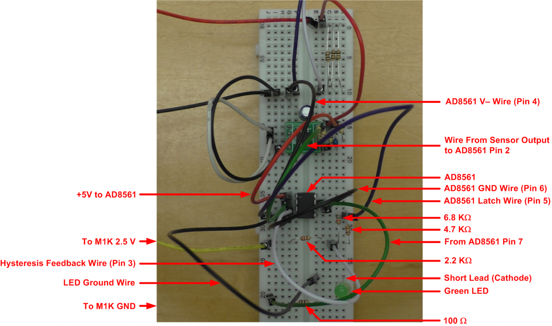
- Add the following Hall effect sensor circuit to the solderless breadboard

- Refer to the illustration below for one way to install the Hall effect sensor components in the solderless breadboard

- Run PixelPulse on the computer and plug in the M1K using the supplied USB cable
- Update M1K firmware, if necessary
- Connect the M1K to the circuit as indicated in the schematic
- Set up PixelPulse to measure voltage on Channel A and deselect repeated sweep mode in the tools menu
- Observe and record the DC voltage on Channel A with the electromagnet far from the sensor chip and define this as VOUT,Z
- This voltage is ideally mid-supply, which is 2.5V on a 5.0 V supply, but it will differ from mid-supply due to DC offsets in the sensor and op-amp that get multiplied by the op-amp closed-loop gain; the output offset voltage may be changed by adding a resistor R4 between the 5.0 V supply and the op-amp summing node on Pin 6.
- Refer to the following schematic for the placement of R4, but do not install any resistor here at this time

- Calculate the op-amp closed-loop gain
- Our objective is to place the sensor output voltage with no applied magnetic field as close as possible to the lower end of its linear range, which is 0.5 V. We calculate the value of R4 in the next few steps. It's important to note that the 5.0 V supply will actually be at about 4.8 V due to the IR drop (internal to the M1K) that is produced by the 150 mA current that drives the electromagnet and that the resistor values are limited and have +/-5% tolerances, so the final voltage will not be perfect. We will therefore use 2.4 V for the mid-supply voltage.
- In order to calculate R4 it is necessary to know the currents flowing in and out of the op-amp summing node. The current through R2 is defined as IR2. Under ideal conditions this current would be zero since the voltage on each side of it would be mid-supply, but there is a small offset voltage between the internal Hall effect sensor output voltage with zero field and the internally buffered VREF. For small gains this voltage can in many instances be ignored, but it must be considered in high-gain circuits such as this one.
- Use the M1K to measure and record the voltage at Pin 7 and define it as VREF
- Use the M1K to measure and record the voltage at Pin 6 and define it as VCM; this is the common-mode voltage at the op-amp input, and is driven to be very close to the output of the internal Hall effect sensor by negative feedback
- Calculate the voltage across R2, VR2, as VR2 = VREF - VCM.
- Calculate the current through R2 as IR2 = VR2/235 Ω
- Calculate the current through the feedback resistor R3, IR3, as IR3 = (VCM - VOUT,Z)/100 KΩ
- Note that these two currents are not exactly equal; can you explain why?
- Calculate the amount of voltage shift, VSHIFT, necessary to move VOUT,Z from its current level down to 0.5 V as VSHIFT = 0.5 V - VOUT,Z; note the VSHIFT is a negative quantity
- Calculate the amount of additional current, ISHIFT, required through the feedback resistor R3 to shift VOUT,Z to 0.5 V as ISHIFT = VSHIFT/100 KΩ; note that this is a negative quantity because VSHIFT is negative
- The current flowing into the summing node through R4, IR4, that is used to create the desired offset is in the opposite direction to that of ISHIFT, so we can write IR4 = -ISHIFT, which is a positive quantity
- Calculate the value of R4 by noting that the voltage across R4 is the difference between the supply voltage, which we determined to be 4.8 V, and VCM, as R4 = (4.8 V - VCM)/IR4
- Select a resistor from the kit that is closest to this value for R4; unless the calculated value is very close to a value available in the kit, round up in order to make any error result in a higher output voltage
- Place R4 in the circuit as shown in the schematic above
- Refer to the illustration below for one way to install R4 in the solderless breadboard

- Verify that VOUT,Z has shifted down to approximately 0.5 V, and that there is some error in this due to supply voltage uncertainties, imperfect R4 value, and resistor tolerances
- Remove the 0.1 μF capacitor and observe the increase in noise on VOUT,Z; can you explain why this happens?
- Replace the 0.1 μF capacitor and observe the reduction in noise on the output voltage
- Slowly move the electromagnet close to the top of the sensor chip until the top of the inductor touches the top of the chip
- Observe the direction of the change in voltage
- Change the orientation of current flow in the inductor if necessary in order to cause the sensor output voltage to increase as the electromagnet moves closer to the sensor (Explain what is happening here.)
- Move the electromagnet again such that the top side of the inductor is touching the top if the AD22151 chip and maneuver it to obtain the highest output voltage reading and record this as VOUT,MAX
- Take the average of the VOUT,Z and VOUT,MAX readings and record this as VOUT,AVG
- Add the following comparator circuit to the solderless breadboard

- Refer to the illustration below for one way to install the comparator circuit
- Slowly move the electromagnet toward the top of AD22151 sensor and observe position where the LED turns on
- Slowly move the electromagnet away from the AD22151 sensor and observe the position where the LED turns off
- Notice that the LED turn and turn off behaviors are very abrupt and there is no intermediate state in which the LED appears to be partially on
- Monitor the comparator threshold voltage on Pin 3 of the AD8561 on Channel A while moving the electromagnet
- Carefully observe and record the threshold voltage at which the LED turns on
- Carefully observe and record the threshold voltage at which the LED turns off
- Can you explain why there are two different threshold voltages and how having two threshold voltages provides an advantage in this binary proximity detector?


Theory
Most magnetic-field-based proximity sensors use strong permanent magnets to generate the magnetic fields that are sensed, and therefore the sensors only require modest gains in order to output a reasonable voltage. In this lab we generate a relatively weak magnetic field using an electromagnet carrying about 150 mA, and thus require a fairly large gain in the op-amp contained in the Hall effect sensor. Having large op-amp gain introduces a few practical problems. One problem is that the output noise is large. This happens because the noise at the input to the op-amp gets multiplied along with the desired signal in the op-amp and appears at the op-amp output. Another similar problem is DC offset, in which a small offset at the input to the op-amp gets multiplied by the op-amp and appears as a DC offset on the output voltage. The op-amp itself has an input offset voltage, imperfectly matched input bias currents that get converted to voltages which are reflected to the op-amp output voltage, and the internal Hall effect sensor output offset and internally generated and buffered reference voltage, REF, are not exactly the same. These all contribute to the output offset voltage, and are the reasons why the output voltage is not exactly at mid-supply when no magnetic field is present. We can compensate for these offsets, and even shift the output offset voltage wherever we need to (within the limits of the part) by summing in an offset voltage at the op-amp's summing node.
The summing node of the op-amp contained in the AD22151 is made available on Pin 6, and the non-inverting op-amp input is internally biased at approximately +2.5 V, so it is possible to inject positive or negative current into the summing node in order to shift the output offset level. In this case we desire to shift the output offset down, which requires an injection of current into the summing node. This can also be viewed as summing a positive voltage into an inverting op-amp summing amplifier configuration. With zero magnetic field applied, the voltage across the op-amp gain resistor R2 is ideally zero since the reference voltage VREF and the output of the Hall effect sensor would be the same -- note that the voltage on the op-amp inverting input is driven to be essentially the same as the voltage no the non-inverting input by negative feedback, so the voltage on the inverting input can be viewed as essentially the same as that of the Hall effect sensor output, neglecting the op-amp input offset voltage. The voltage that is essentially common to both op-amp inputs is referred to as the “input common-mode voltage.” There is, however, a small voltage across R2 due to the mismatch between VREF and the op-amp input common-mode voltage. Even though this is a small voltage, it is applied across a small resistance and produces an appreciable current that flows through a large-valued feedback resistor to produce an appreciable shift in output voltage. This is how op-amps work to amplify signal voltages, and why the inverting gain of an op-amp is proportional to the feedback resistance and inversely proportional to the gain resistance. We can determine the current flowing though R2 by measuring the voltage across it and dividing by its value. Most of this current flows through the feedback resistor R3, but a small amount flows into the op-amp inverting input; this small current is the input bias current, and is the reason why the current through R2 is not exactly equal to the current through R3.
Additional current can be added through the feedback resistor in order to shift the output voltage down to the lower end of its linear range of 0.5 V. The amount of current necessary for this can be calculated by taking the difference between the existing output voltage and the desired output voltage and dividing by the feedback resistance. This value of current is then injected into the op-amp summing node through an offset injection resistor R4. The value of R4 is calculated as the difference between the voltage on the input side of R4 (we used 4.8 V for this) and the op-amp input common-mode voltage divided by the required injection current.
The op-amp is set up as a non-inverting amplifier to the voltage that is output from the Hall effect sensor element. The gain of a non-inverting op-amp, AV,NI, is the ratio of the feedback resistance to the gain resistance plus one. In terms of the reference designators used in the lab, this is AV,NI = 1 + R3/R2. Note that VREF is also summed in an inverting fashion in order to place the output nominally at mid-supply (it is close to mid-supply for the typical small gains that are used when permanent magnets are used as the sources of the magnetic fields). The gain of an inverting op-amp, AV,I, is the negative of the ratio of the feedback resistance to the gain resistance, or AV,I = -R3/R2. The output level with no magnetic field present has been defined by the gain, circuit offsets, VREF, and the offset injection circuitry. The AD22151 output voltage, VO, due to the Hall effect sensor element output voltage, VH, is therefore simply
The gain from VH to VO is 1 + R3/R2, and in this lab is approximately equal to 427. This is a relatively high gain, which amplifies the noise from the Hall effect sensor element to a level that is visible on the PixelPulse voltage display. Placing the 0.1 μF capacitor across the feedback resistor reduces the non-inverting gain as frequency increases because the reactance of the capacitor decreases with frequency, thereby reducing the overall feedback impedance as frequency increases (the general gain formula for a non-inverting op-amp is AV,NI = 1 + ZF/ZG where ZF and ZG are the feedback and gain impedances, respectively). The feedback impedance can only approach a minimum of zero, and therefore the minimum gain of a non-inverting op-amp is equal to 1 + 0 = 1. This means that the noise from the Hall effect sensor element cannot be attenuated in the non-inverting amplifier. An inverting amplifier, on the other hand, can attenuate signals applied to its input, and is therefore a better configuration to be used in filtering applications. The capacitor across the feedback resistor therefore does help somewhat to reduce noise, but cannot reduce the op-amp gain below one. Removing the feedback capacitor eliminates the high frequency gain reduction, and allows us to see the unfiltered noise on the PixelPulse display.
Series RC circuits can realize the simplest lowpass and highpass filters that operate on voltages, though current-mode operation is also possible. The filter is lowpass when the output voltage is taken across the capacitor and is highpass when the output voltage is taken across the resistor. The filter operates as a two-element voltage divider between the resistance of the resistor, R, and the reactance of the capacitor, 1/2πfC. Since the capacitive reactance varies inversely with frequency, the voltage across the capacitor decreases with frequency, producing the lowpass frequency response. By Kirchhoff's Voltage Law, the voltage across the resistor increases with frequency in a complementary fashion to that of the capacitor, producing the highpass response. The cutoff frequency fC is defined as the frequency at which the capacitive reactance is equal to the resistance. Setting R = 1/2πfCC and solving for fC gives the following result.
At the cutoff frequency, the amplitude of the sinusoidal output voltage in response to a sinusoidal input voltage is equal to the reciprocal of the square-root of two times the input voltage amplitude, or about 70.7% of the input voltage amplitude.
The lowpass filter in the lab is comprised of a 68 Ω resistor and a 22 μF capacitor, and therefore has a cutoff frequency of approximately 106 Hz. Because of the tolerances of the resistor and capacitor, the actual cutoff frequency will deviate from this value. The frequency at which the peak-to-peak output amplitude was measured to drop from about 5 V to (0.707)*5 V ≈ 3.5 V in the lowpass filter part of the lab should have been close to 106 Hz.
The highpass filter in the lab is comprised of a 68 Ω resistor and a 10 μF capacitor, and therefore has a cutoff frequency of approximately 234 Hz. As with the lowpass filter, component tolerances will introduce a small cutoff frequency error. The frequency at which the peak-to-peak output amplitude was measured to drop from about 5 V to (0.707)*5 V ≈ 3.5 V in the highpass filter part of the lab should have been close to 234 Hz.
It's important to note that the resistor in the highpass filter is referenced to +2.5 V instead of ground. The highpass filter cannot pass DC, and it can therefore be viewed as a circuit the removes the DC level from its input signal. The DC level on the other side of the resistor sets the DC level on the output side of the highpasss filter as long as the output does not have a significant DC load. This is true because DC current cannot flow back through the capacitor and there is no significant load current, so the DC voltage drop across the resistor in the highpass filter is effectively zero. Placing the output DC level at 2.5 V places the output swing in the center of the M1K input range. If the resistor were referenced to ground, the highpass filter output would swing above and below ground, and the negative excursions would not be visible on the M1K.
After making basic characterizations of the filters, simple, rather inaccurate, peak detectors consisting of series diodes and shunt capacitors are added to the filter outputs in order to give a rough indication of the filter output level. The peak detector allows the capacitor to charge when the voltage out of the filter is greater than the capacitor voltage plus the forward diode drop. The diode is a nonlinear element with a varying forward voltage drop, so the capacitor will not be able to charge to the actual peak voltage out of the filter. Once the signal out of the filter passes its peak, the diode becomes reverse-biased and conducts very little current, allowing to the capacitor to hold a rough estimate of the peak level that includes the error due to the diode drop. The capacitor voltage does not stay perfectly constant while the diode is reverse biased because the diode leaks current when reverse biased, and current leaks into the M1K when the when the capacitor voltage is measured. The current leakages cause the capacitor voltage to sag during reverse-biased parts of the cycle. The sag is more noticeable for low frequency inputs when the reverse-biased times are long. This brings up an important dilemma that is encountered in all peak detectors. A small capacitor is desirable for fast charging times required in detecting the peaks of high frequency signals, but a large capacitor is required to achieve long hold times for low frequency signals. Ultimately, a compromise must be reached in selecting the capacitor value in a given application. Much more accurate peak detectors can be built using negative feedback circuits that remove the diode drop error from the measurement.
Since these peak detectors include errors, it is best to measure their outputs for various levels output from the filters. In the lab, frequencies roughly a quarter-decade apart are used to characterize the peak detectors. One of these frequencies is chosen to be approximately equal to the cutoff frequency of the respective filter -- 100 Hz for the lowpass filter and 200 Hz for the highpass filter. These peak detector output levels are used to set the threshold levels of the comparators that detect when the signals are in the filter passbands and drive the corresponding LEDs.
A comparator is a high-gain amplifier with a differential input and a binary output that is used to detect when input signals are above or below a predetermined threshold voltage. A comparator is similar to an operational amplifier that is set up in an open-loop configuration, though operational amplifiers should not be used as comparators for a number of reasons. There are many comparators on the market that are specifically designed to be operated open-loop and provide a specific type of digital logic output. Comparators can also be operated in a closed-loop positive-feedback configuration to produce hysteresis. Hysteresis is a feature in which the operation of the comparator depends on its history. It provides two thresholds -- a higher one for increasing inputs and a lower one for decreasing inputs. One of the major benefits of hysteresis is that it prevents the comparator output from “chattering” when the input signal is changing very slowly about the threshold. Hysteresis would be a nice feature in this application if the input frequencies were hovering near the filter cutoff frequencies, but it was not included for simplicity's sake.
The comparators are set up with threshold voltages on their inverting inputs. The output logic goes to a “high” level when the voltage on the non-inverting input exceeds the threshold voltage by a small amount. We want to drive the LED when the threshold is exceeded, indicating that the input signal is in the filter passband, and it is best to drive the LED when the comparator output is in the “low” logic state. The AD8561 has true and complimentary outputs. The true output goes high when the input voltage exceeds the threshold voltage is exceeded and low when the input voltage is below the threshold voltage. The complementary output beaves in the opposite fashion. Since the complementary output goes “low” when the input voltage exceeds the threshold voltage, it is used to drive the LED. If the comparator only had a true output, the same result could be achieved by swapping the input signals, i.e., placing the threshold voltage on the non-inverting input and the input signal on the inverting input.
Observations and Conclusions
- An electric filter is a circuit that passes certain frequencies and rejects other frequencies
- The simplest filters consist of two elements, RC and RL
- A lowpass filter passes low frequencies and rejects high frequencies
- A highpasss filter passes high frequencies and rejects low frequencies
- A highpass filter does not pass DC
- RC and RL circuits can each be designed as simple lowpass or highpass filters
- The passband of a filter is commonly defined as the band of frequencies for which the amplitude of the output signal ranges from 100% to 70.7% of the input amplitude
- The end of the passband is called the cutoff frequency, fC
- A simple, low-accuracy peak detector can be constructed using a diode and a capacitor
- The diode drop introduces errors in the simple peak detector
- A tradeoff must be made when selecting a capacitor for a peak detector -- smaller is better for high frequencies and larger is better for low frequencies
- A comparator is a high-gain amplifier that is often used to provide a binary output indicating whether an input signal is above or below a predetermined threshold
- Operational amplifiers should not be used as comparators
university/courses/engineering_discovery/lab_6.1466621508.txt.gz · Last modified: 22 Jun 2016 20:51 by Jonathan Pearson