


This version is outdated by a newer approved version. This version (19 Oct 2016 17:28) was approved by Jonathan Pearson.The Previously approved version (05 Oct 2016 23:09) is available.
This version (19 Oct 2016 17:28) was approved by Jonathan Pearson.The Previously approved version (05 Oct 2016 23:09) is available.This is an old revision of the document!
Table of Contents
Class A NPN Emitter-Follower Amplifier
VideoNumberHere
Introduction
The common-emitter amplifier introduced in the “Class A NPN Common-Emitter Amplifier” lab provided voltage and current amplification, but suffered from a large output resistance that was equal to the equivalent collector resistance that was present for AC signals. The emitter-follower, EF, also called common-collector, CC, amplifier provides nearly unity voltage gain and current gain, which can be large, and low output resistance. Emitter-follower amplifiers are commonly used as output stages that are capable of driving low impedance loads due to their current gains and low output resistances. The name “emitter-follower” originates from the fact that the output signal, taken at the emitter, follows the input signal, applied at the base, with nearly unity gain. “Emitter-follower” is more descriptive than “common-collector,” and will be used henceforth for this reason. As with the CE amplifier, we will study the EF amplifier using a single transistor biased in a Class A configuration.
Unlike the CE amplifier, the output voltage and input voltage of an EF amplifier are in-phase with each other and of nearly the same magnitude. This is the sense in which the output voltage at the emitter “follows” the input. The collector is generally connected directly to the power supply and the emitter is connected to another supply voltage -- often ground -- through an emitter resistor, RE. The operation of an EF amplifier constitutes a form of negative feedback. Negative feedback systems are discussed in further detail in later labs, but can be briefly described as systems in which part or all of an output quantity is fed back upstream in the system in such a way as to reduce an error that exists between the existing condition and the desired condition. Automotive cruise control is an example of an everyday negative feedback system in which the speed of an automobile is constantly monitored and adjusted in such a way as to minimize the error between the current speed and the speed set by the driver. Negative feedback systems are often used to regulate physical phenomena. Reference to the schematic in the Procedure section of the lab will be helpful when reading the remainder of this section. In the emitter-follower amplifier, the negative feedback occurs as follows: starting at the emitter, as the emitter voltage vE increases, the base-emitter voltage vBE decreases, which in turn reduces the base current iB, which reduces the collector current iC by the iC = βiB relationship; recalling that for large β we can say that iE ≈ iC (the exact relationship between iE and iB) is iE = (1 + β)iB, and (1 + β)iB ≈ βiB for large β) we see that iE decreases as iC, thuis reducing vE. This negative feedback action regulates the bias point and voltage gain of the emitter-follower, keeping the voltage gain close to unity. This same feedback loop helps regulate the operating bias point in the CE amplifier. In many, if not most, applications, we can view the emitter follower as having unity voltage gain with the output voltage shifted down from the input voltage by one vBE drop. The bias point considerations for the Class A emitter-follower amplifier are the same as for the Class A CE amplifier.
The current gain and low output impedance of the emitter-follower amplifier make it ideal for driving low impedance loads, which may be DC- or AC-coupled. Many amplifiers are designed with emitter-follower output stages placed after voltage gain stages. In this lab we design, build, and evaluate a single Class A emitter-follower amplifier, then place it after the CE amplifier used in the Class A NPN Common-Emitter Amplifier lab in a DC-coupled fashion to illustrate how it can be used to drive an AC-coupled load much heavier than the 1 KΩ load used in that lab, and that it eliminates the gain loss due to the loading of the high output resistance of the CE stage. An example of how an emitter-follower stage can be added to an operational amplifier “inside the loop” to drive a low impedance loudspeaker is shown in the “Audio Amplifier with Electret Microphone” lab.
Objective
To design, build, and test an emitter-follower amplifier using a 2N3904 NPN transistor, with an input resistance of at least 1 KΩ that is capable of driving an AC-coupled 47 Ω load with a 2 VP-P sine wave. To increase the load to 10 Ω and observe that this heavier load can still be driven, limited by the available current. To verify that the amplifier has approximately unity gain and that the Q-point is close to its designed value. To observe the buffering effect of the emitter follower and show how output loading is minimal as compared with a CE amplifier. To understand and be able to calculate emitter-follower amplifier voltage gain, power gain, efficiency, and power dissipation. To append the emitter-follower stage to the output of the CE amplifier designed in the “Class A NPN Common-Emitter Amplifier” lab in a DC-coupled fashion to show how buffers are added to voltage gain stages in order to drive low impedance loads. Following completion of this lab you should be able to explain the basic operation of an emitter-follower amplifier, explain how negative feedback stabilizes the gain of a common-emitter amplifier, explain why output loading does not affect an emitter-follower amplifier nearly as much as a CE amplifier, and calculate the amplifier voltage gain, power gain, efficiency, and power dissipation of a Class A emitter-follower amplifier.
Materials and Apparatus
- Data sheet handout for the 2N3904 NPN transistor
- Computer running PixelPulse software
- Analog Devices ADALM1000 (M1K)
- Solderless breadboard and jumper wires from the ADALP2000 Analog Parts Kit
- (2) 2N3904 NPN transistor from the ADALP2000 Analog Parts Kit
- (1) 10 Ω resistor from the ADALP2000 Analog Parts Kit
- (1) 47 Ω resistor from the ADALP2000 Analog Parts Kit
- (1) 68 Ω resistor from the ADALP2000 Analog Parts Kit
- (2) 100 Ω resistor from the ADALP2000 Analog Parts Kit
- (1) 470 Ω resistor from the ADALP2000 Analog Parts Kit
- (1) 1 KΩ resistor from the ADALP2000 Analog Parts Kit
- (1) 1.5 KΩ resistor from the ADALP2000 Analog Parts Kit
- (2) 4.7 KΩ resistor from the ADALP2000 Analog Parts Kit
- (1) 6.8 KΩ resistor from the ADALP2000 Analog Parts Kit
- (2) 47 μF capacitor from the ADALP2000 Analog Parts Kit
- (1) 220 μF capacitor from the ADALP2000 Analog Parts Kit
Procedure
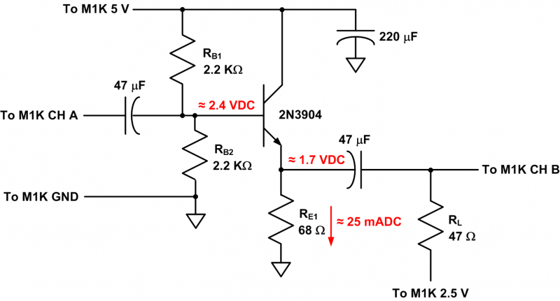
- Construct the following circuit on the solderless breadboard
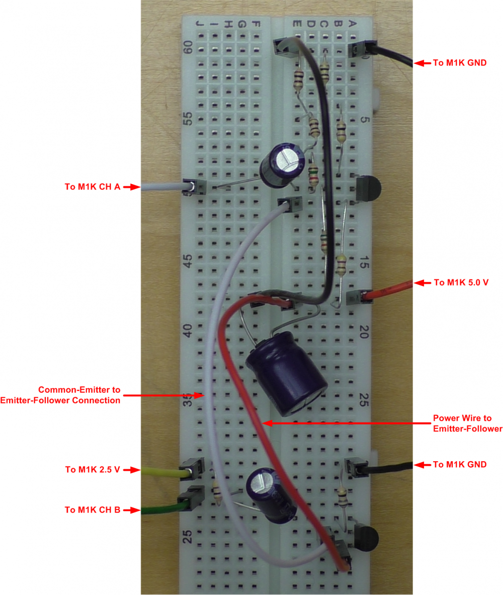
- Refer to the illustration below for one way to install the components in the solderless breadboard. Note that this circuit has been added to the CE amplifier breadboard from the “Class A NPN Common-Emitter Amplifier” lab.

- Run PixelPulse and plug in the M1K using the supplied USB cable
- Update M1K firmware, if necessary
- Disable “Repeated Sweep” mode; waveforms can be paused for analysis
- Set up the M1K to source voltage/measure current on Channel A and measure voltage on Channel B
- Set up Channel A source waveform for a 100 Hz “Sine” output that swings between 2.0 V and of 4.0 V
- Observe the output voltage into the 1 KΩ load resistor on Channel B and verify that it is swinging nominally +/- 1 V about the 2.5 V baseline and that it is in-phase with the input signal
- Observe the voltage at the emitter on Channel B and verify that it is swinging nominally +/- V about a 1.7 V bias voltage and that it is also in-phase with the input signal. Note that these voltages may vary somewhat due to resistor tolerances
- Note any visible distortions in the output signals
- Remove the input signal and measure the DC bias voltages at the base, emitter, and collector, and verify that these are at their designed levels, allowing for resistor tolerances
- Calculate the voltage gain, power gain, and efficiency of this amplifier; compare the power dissipation of this circuit with that of the CE amplifier in the “Class A NPN Common-Emitter Amplifier” lab
- Set up Channel A source waveform for a 100 Hz “Sine” output that swings between 2.3 V and of 2.7 V
- Remove the AC-coupling capacitor and bias resistors from the amplifier input and connect it to the output of the CE amplifier from the “Class A NPN Common-Emitter Amplifier” lab as shown in the schematic. Note the change in the emitter-follower bias point
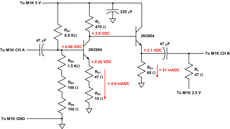
- Refer to the illustration below for one way to interconnect the two amplifiers on the solderless breadboard
- Verify that the voltage across the 47 Ω load resistor is swinging +/- 1V about the 2.5 V bias voltage
- Calculate the rms power dissipation in the load resistor
- Estimate the voltage swing that would be present across the 47 Ω load resistor if it were driven by the CE stage alone, without the emitter-follower buffer in place
- Reduce the swing of the input voltage to 2.45 V to 2.55 V
- Replace the 47 Ω load resistor with a 10 Ω resistor
- Verify that the output voltage swings 500 mVP-P about the 2.5 V bias voltage
- Calculate the load current into the 10 Ω load resistor


Theory
The emitter-follower amplifier presents a high input resistance to signals applied to its base and provides a low resistance effective voltage source at its output. These characteristics make the emitter-follower amplifier well suited for use as a voltage buffer amplifier. Buffer amplifiers are used to buffer heavy loads from signal sources that have a high output resistance. A good buffer has a high input resistance so as not to significantly load the output resistance of the source that is being buffered and a low resistance voltage source output that is capable of driving heavy loads with minimal loading loss.
Our amplifier needs to drive a 47 Ω load with a +/-1 V sine wave, which requires approximately +/-21 mA. We will make the base bias point at about mid-supply. Starting with a mid-supply base bias voltage, we can estimate the emitter voltage to be 2.5 V - 0.7 V = 1.8 V. We have a 68 Ω resistor in the kit, and if we use this for our RE, we get an emitter current of 1.8 V/68 Ω ≈ 26.5 mA. This exceeds our minimum current of 21 mA, so we will start with this. If we want to make a first-round estimate of the voltage drop incurred due to base current, remembering that iE ≈ iC, we use β = 200 to estimate the base current as iB ≈ 26.5 mA/200 ≈ 133 μA. The base bias current is on the high side because we are using a large emitter current. The voltage drop due to the base current can be estimated to be (133 μA)(2.2 KΩ||2.2 KΩ) ≈ 0.15 V. This reduction will in turn reduce the emitter voltage, which will reduce the emitter current, which will reduce the base current and its associated voltage drop, so a reasonable estimate for base bias voltage reduction due to base bias current would be about 0.1 V, so we will use 2.4 V for the base voltage. Now, a more accurate emitter bias voltage can be established as 2.4 V - 0.7 V = 1.7 V. The emitter bias current can be calculated as 1.7 V/68 Ω = 25 mA.
The input resistance looking into the base of the transistor used in the emitter-follower amplifier Ri,base is the same as that of the CE amplifier
Using β = 200 from the Introduction to Transistors lab, and substituting numbers from this lab, we have
When we use the voltage divider to provide base bias, we need to include the resistors in the divider in parallel with the input resistance looking into the base, so the total input resistance Riis
Note that this result falls slightly short of our design goal of having a minimum input resistance of 1 KΩ. This is primarily due to the 2.2 KΩ resistors that were used to set up the base bias voltage. We could increase the value of these resistors a small amount and raise the input resistance to at least 1 KΩ, but the next largest value in the kit is 4.7 KΩ, which would give us considerably more unnecessary voltage drop on the base bias voltage. The best solution, if all commercially available resistor values were available, would be to use the smallest available resistor value that meets the input resistance requirement.
For large β (≥ 100) the output resistance looking into the emitter of the emitter-follower amplifier Ro is calculated as
where RS is the total equivalent source resistance in the base circuit. In our circuit, RS is equal to the parallel combination of the base bias resistors and the source resistance feeding the base. Note that when the emitter-follower amplifier is fed by the low resistance voltage source output of the M1K, RS ≈ 0 and the output resistance is simply the incremental emitter resistance re.
When we place the emitter-follower on the output of the CE amplifier from the “Class A NPN Common-Emitter Amplifier” lab, we have nonzero RS, and need to include it in out calculation of Ro
We will see a small voltage divider loss when driving the 47 Ω load, and a more pronounced loss when driving the 10 Ω load. With the emitter-follower amplifier buffering the CE amplifier, we will have voltage divider factors of 47 Ω/49.6 Ω ≈ 0.95 for the 47 Ω load and 10 Ω/12.6 Ω ≈ 0.79 for the 10 Ω load.
We can calculate the efficiency of the emitter-follower amplifier studied in this lab.
For the emitter-follower amplifier by itself driving +/-1 V into the 47 Ω load resistor, the power into the load is:
Note that the power into the load could also have been calculated using the [vLOAD(rms)]2/RL formula.
The quiescent power drawn from the supply is:
The efficiency is therefore:
For the emitter-follower amplifier buffering the CE amplifier driving +/-1 V into the 47 Ω load resistor, the power into the load is again:
The total quiescent power drawn from the supply, using the results already calculated in the CE amplifier lab, is:
The efficiency is therefore:
If we substitute the 10 Ω load for the 47 Ω load, we can only deliver about +/- 0.25 V to the load, and the power into the load is
The efficiency is now only
It is important to note that the voltage divider losses between the emitter-follower output and the load were omitted.
We can calculate the power gain of the two cascaded amplifiers with the 47 Ω load using the results obtained in the “Class A NPN Common-Emitter Amplifier” lab. The voltage gain is essentially the same as it was for the CE amplifier because the voltage gain of the emitter-follower amplifier is very close to unity and the input resistance of the CE is unchanged. The power gain is therefore
From this result, we can see how adding the emitter-follower output stage increased the overall power gain by providing current gain to drive the heavier load.
Observations and Conclusions
- Emitter-follower amplifiers provide significant current gain and unity voltage gain
- The operation of an emitter-follower amplifier involves a form of negative feedback
- Emitter-follower amplifiers have high input resistance and low output resistance
- Emitter-follower amplifiers are often used to buffer heavy loads that require large output currents from sources that have high source resistances
- Adding an emitter-follower stage to a CE amplifier can significantly increase the power gain of the overall amplifier
university/courses/engineering_discovery/lab_11.1476890882.txt.gz · Last modified: 19 Oct 2016 17:28 by Jonathan Pearson