


This version (03 Jan 2018 19:38) was approved by Doug Mercer.The Previously approved version (21 Oct 2016 22:04) is available.
Table of Contents
Class A NPN Common-Emitter Amplifier
5179788276001
Introduction
The basic operation of the NPN transistor was introduced in the “Introduction to Transistors” lab. In this lab we build and evaluate a Class A amplifier using a NPN transistor and a few passive elements. Initial amplifier configurations were divided into classes based upon the angle of a sine wave being amplified in which the transistor was operational. This angle is called the conduction angle. In Class A amplifiers, the transistor is operational over the full sine wave cycle, so its conduction angle is 360 degrees. This type of operation produces relatively low distortion, mostly limited to the distortion of the transistor itself, but is also low on efficiency since the transistor dissipates considerable DC power even when there is no input signal present. We will delve further into the efficiency of Class A amplifiers in the Theory section. The three commonly-used Class A bipolar transistor configurations are the common-emitter (CE), emitter-follower (EF) (sometimes called common-collector, CC), and common-base (CB) amplifiers. Other classes include amplifiers with conduction angles less than 360 degrees, amplifiers that use pulsed digital signals followed by lowpass filters, and amplifiers with power supply voltages that track the signal being amplified in order to maximize efficiency. We investigate the CE configuration in this lab, which is capable of voltage and current amplification, and is likely the most widely-used Class A amplifier configuration. Reference to the schematic in the Procedure section of the lab will be helpful when reading the remainder of this section.
The CE amplifier is generally used as a voltage amplifier, and the phase of its output voltage is inverted with respect to that of its input voltage. The input voltage is applied to the base and the output voltage is taken from the collector; most often these voltages are measured with respect to a ground, or zero volt, reference. As the base current increases, the collector current increases as a factor of β multiplied by the base current. The collector current flows through a collector resistor RC connected between the collector and a DC power supply, producing a voltage drop across RC. This action causes the collector voltage to drop as the voltage applied to the base increases, thereby producing an output voltage that is 180 degrees out-of-phase with the input voltage.
All Class A amplifiers require a DC bias to set the quiescent point, or Q-point at which the amplifier operates. The quiescent point is defined as the transistor's DC collector current IC and collector-to-emitter voltage VCE when no input signal is present. When an input signal is applied the collector current and collector-to-emitter voltage increase and decrease, out-of-phase with each other. It is important to ensure that there is sufficient range available for the collector current and the base-emitter voltage, and this is the primary consideration when setting the Q-point. The signals being amplified ride on the DC bias and are often referred to as incremental or signal voltages and currents. DC quantities are represented by variables with upper-case letters with upper-case subscripts, incremental quantities are represented by lower-case letters with lower-case subscripts, and the two together are represented by lower-case letters with upper-case subscripts. This nomenclature is used in small signal transistor modeling in which circuit behavior with small, incremental signals is analyzed around a particular Q-point.
The inputs and outputs of Class A amplifiers can be either DC- or AC-coupled. When DC-coupled, the DC voltage of the source that is feeding the amplifier input must match the DC bias voltage required by the amplifier input, and similarly, the DC voltage of the output must match the DC voltage requirement of the input of whatever the amplifier is feeding. Often several Class A amplifier stages are DC-coupled together in a cascade, and the inter-stage DC levels are designed to be compatible with one another. AC-coupling is simpler in that each stage can have its own bias configuration, independent of the other stages, but AC-coupled systems do not pass DC, which is often a requirement. In this lab we build a simple AC-coupled CE amplifier stage and use it to amplify a voltage and drive an AC-coupled 1 KΩ load.
The gain of a CE amplifier can be precisely calculated using circuit analysis, but it can also be estimated by simply inspecting the circuit. In the simplest CE amplifiers, a single emitter resistor RE is connected between the emitter and a voltage lower than that connected to RC, often the system ground. This resistor forms part of the transistor's bias network and also plays a part in determining the gain of the amplifier. As we learned in the “Introduction to Transistors” lab, we can estimate the emitter and collector currents to be approximately equal to each other. If RE is connected between the emitter and system ground, the signal voltage across RE will be a close replica of the voltage applied to the base, only shifted down by approximately 0.7 VDC -- the standard base-emitter drop we learned about in the “Introduction to Transistors” lab. This signal voltage produces a current in RE that is approximately equal to vi/RE, where vi is the input voltage to the amplifier. This is the emitter signal current ie, which is approximately equal to the collector signal current ic, which flows through RC. From this we can see that the collector signal voltage vc, which is also the output voltage vo is equal to -icRC. Combining these results we get -vo = vi[RC/RE], and the gain vo/vi = -RC/RE. The minus sign indicates the 180 degree phase inversion that exists between the input and output signal voltages. In the lab we will see how to set the bias point as required by the load, and how loading affects the overall amplifier gain. We will see that the large output resistance of the CE amplifier causes an undesirable voltage drop when the amplifier is driving a load, and why another low-output resistance stage is often added to CE amplifiers that drive moderate to heavy loads.
Objective
To design, build, and test a CE amplifier, using a 2N3904 NPN transistor, with a loaded voltage gain of -5 and input resistance of at least 1 KΩ that is capable of driving an AC-coupled 1 KΩ load with a 2 VP-P sine wave. To verify that the amplifier Q-point and gain are close to their designed values. To observe the effects of loading on a CE amplifier output. To understand and be able to calculate CE amplifier voltage gain, power gain, and efficiency. Following completion of this lab you should be able to give the definition of a Class A amplifier and explain the basic operation of a CE amplifier, explain what a Q-point is, explain how output loading affects the overall voltage gain of a CE amplifier, and calculate the amplifier voltage gain, power gain, and efficiency of a CE amplifier.
Materials and Apparatus
- Data sheet handout for the 2N3904 NPN transistor
- Computer running PixelPulse software
- Analog Devices ADALM1000 (M1K)
- Solderless breadboard and jumper wires from the ADALP2000 Analog Parts Kit
- (1) 2N3904 NPN transistor from the ADALP2000 Analog Parts Kit
- (1) 10 Ω resistor from the ADALP2000 Analog Parts Kit
- (1) 47 Ω resistor from the ADALP2000 Analog Parts Kit
- (2) 100 Ω resistor from the ADALP2000 Analog Parts Kit
- (1) 470 Ω resistor from the ADALP2000 Analog Parts Kit
- (1) 1 KΩ resistor from the ADALP2000 Analog Parts Kit
- (1) 1.5 KΩ resistor from the ADALP2000 Analog Parts Kit
- (1) 6.8 KΩ resistor from the ADALP2000 Analog Parts Kit
- (2) 47 μF capacitor from the ADALP2000 Analog Parts Kit
- (1) 220 μF capacitor from the ADALP2000 Analog Parts Kit
Procedure
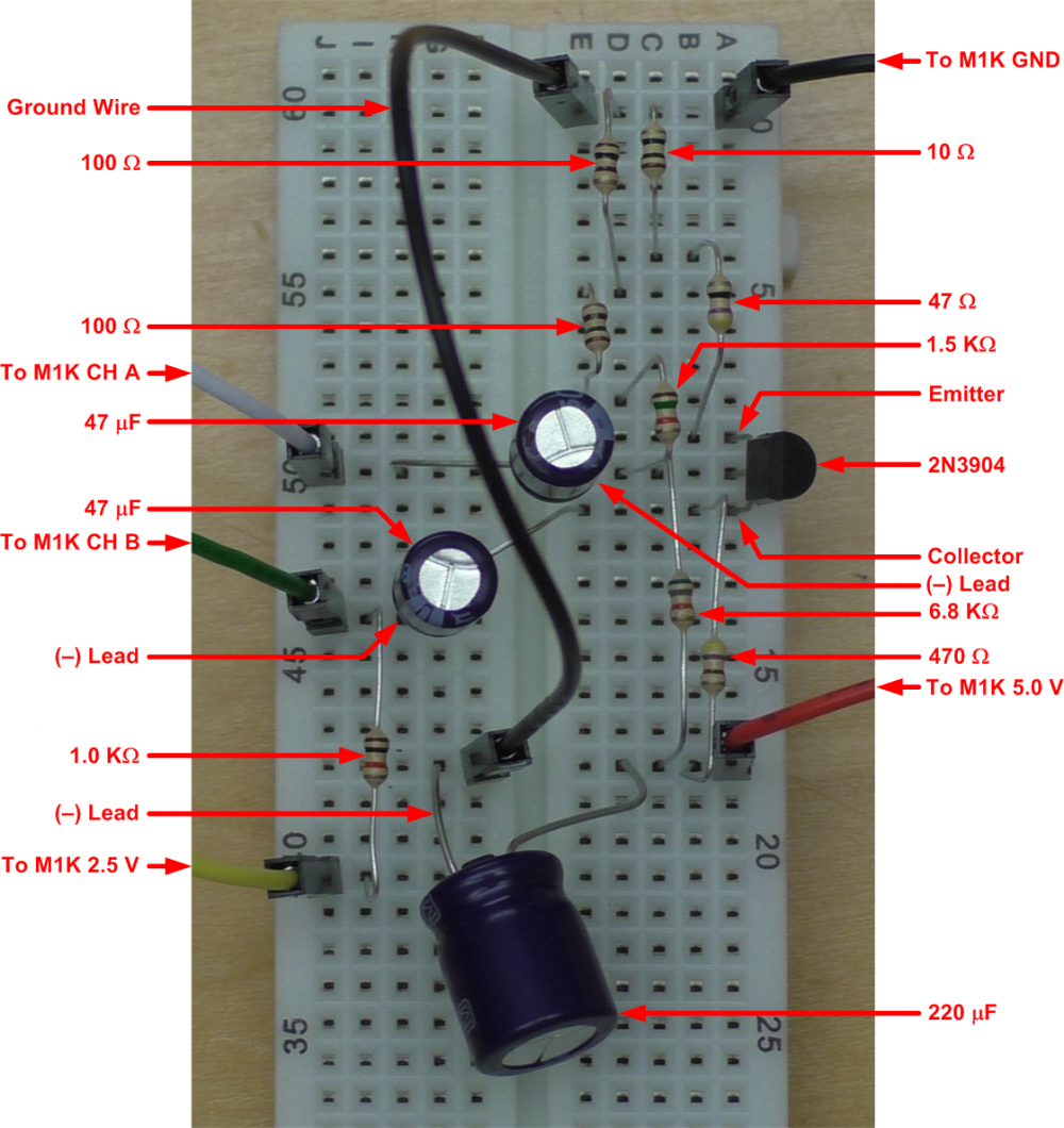
- Construct the following circuit on the solderless breadboard

- Refer to the illustration below for one way to install the components in the solderless breadboard
- Run PixelPulse and plug in the M1K using the supplied USB cable
- Update M1K firmware, if necessary
- Disable “Repeated Sweep” mode; waveforms can be paused for analysis
- Set up the M1K to source voltage/measure current on Channel A and measure voltage on Channel B
- Set up Channel A source waveform for a 100 Hz “Sine” output that swings between 2.3 V and of 2.7 V
- Observe the output voltage into the 1 KΩ load resistor on Channel B and verify that it is swinging nominally +/- 1 V about the 2.5 V baseline and that it is 180 degrees out-of-phase with the input signal
- Remove the 1 KΩ load resistor and observe the voltage at the collector on Channel B and verify that it is swinging nominally +/- 1.47 V about a 2.8 V bias voltage and that it is also 180 degrees out-of-phase with the input signal. Note that these voltages may vary somewhat due to resistor tolerances
- Note any visible distortions in the output signals
- Remove the input signal and measure the DC bias voltages at the base, emitter, and collector, and verify that these are at their designed levels, allowing for resistor tolerances
- Calculate the voltage gain, power gain, and efficiency of this amplifier -- see theory section for details
- This common-emitter amplifier is coupled to the emitter-follower amplifier designed in the “Class A NPN Emitter-Follower Amplifier” lab so it is recommended that this lab remain assembled on the solderless breadboard until completion of that lab


Theory
All Class A amplifiers, no matter what they use for an amplifying device, operate about a Q-point. The amplifier idles at the Q-point until a signal is applied to its input. When an input signal is applied, the amplifier output voltage and current swing up and down according to the input signal. In the CE NPN transistor circuit used in this lab, the voltage across the transistor output and the current flowing in and out of the collector are out-of-phase with each other, i.e., vCE is out-of-phase with iC. We know that in our simple CE amplifier vCE can vary between the supply voltage and the saturation voltage, vCE(sat), which is typically a few tenths of a volt. In normal applications, we do not run the output voltage right up to these limits, but instead allow for some margin in order to prevent serious output signal distortion. Also, it is important to remember that the collector-emitter junction in a BJT must always remain reverse-biased in order to operate in the forward active region.
The Q-point is the (vCE, iC) point with no input signal. In order to obtain maximum output voltage swing, it makes sense to set the Q-point vCE halfway between the upper and lower limits, which is typically somewhere near mid-power-supply. The minimum Q-point setting for iC depends on the load current requirements. When the voltage across the load is increasing, the current into the load is increasing and the current into the collector is decreasing. When the voltage into the load reaches its maximum level of approximately the supply voltage, the collector current goes to zero and all of the current from the supply flows into the load. The minimum Q-point collector current must therefore be equal to the amount of collector current that is taken away from the collector current when the voltage into the load swings from its baseline to its maximum level. Our load resistance is AC-coupled, and we are swinging +/- 1 V (2 VP-P) about a 2.5 V baseline into the 1 KΩ load, which requires +/- 1 mA. This means we require a minimum of 1 mA quiescent collector current in the transistor. In practical circuits, we usually make this larger in order to provide margin, and there may be other factors that influence this choice. We know, however, that we cannot have IC < 1 mA.
In our amplifier, the base bias voltage was designed to be approximately 1 VDC using the voltage divider, though it will be a little less than this due to the small, though finite, base current. In many cases we can ignore base current, but we will see in this amplifier that because the emitter voltage is low, a small change in base voltage, which translates to a similar change in emitter voltage, can cause a significant percentage change in collector current. Additionally, the resistors have 5% tolerance, which can introduce additional error in collector current. Using the voltage divider rule, we calculate that without loading, the voltage at the base is 0.2(5 V) = 1 V. In order to estimate the base current, we can estimate the emitter current as (1 V - 0.7 V)/57 Ω ≈ 5.3 mA. Using β = 200 for the transistor, the base current can be estimated to be approximately 5.3 mA/200 = 26.5 μA. This current flows through the parallel combination of the two base bias resistors, so the voltage drop due to base current can be estimated to be (26.5 μA)(6.8 KΩ||1.7 KΩ) ≈ 36 mV. The base voltage, accounting for base current, can now be estimated to be 1 V - 36 mV ≈ 0.96 V. Note that this slightly changes the collector current, which slightly changes the base current, so technically these calculations are iterative, but one iteration is generally sufficient. The emitter current can now be estimated as (0.96 V - 0.7 V)/57 Ω ≈ 4.6 mA. From this example we can see how a small change in base voltage can significantly change the emitter current, and hence collector current, when the emitter voltage is small. We require small base and emitter voltages since we are operating on a relatively low supply voltage of 5 V and need to keep the collector-base junction reverse-biased over the full collector voltage swing. The next step is to estimate the collector bias voltage as 5 V - (4.6 mA)(470 Ω) ≈ 2.8 V. In order to get our required output swing of +/-1 V across the load resistor we will need about +/-1.47 V at the collector to compensate for the amplifier output resistance of 470 Ω being loaded by the 1 KΩ load. This means that the collector voltage will swing between 1.33 V and 4.27 V, which keeps the collector-base voltage reverse-biased and provides sufficient margin to the supply voltage. Note that since we have a reasonably large output swing and are fairly close to the dynamic range limits, we will incur some possibly visible distortion in the output waveform.
The efficiency of an amplifier is defined as the ratio of the power delivered to its load to the power consumed from the power supply. It is the percentage of the total power consumed from the supply that is delivered to the load. Class A amplifiers are not terribly efficient when compared with other amplifier classes, but they are simple and can have less distortion than some of the other classes and therefore remain quite popular in spite of their poor efficiency. We can calculate the maximum theoretical efficiency of an ideal Class A amplifier driving a capacitively coupled resistive load (for mathematical simplicity, we will reference the load voltage to ground so that the voltage across the load swings above and below ground). To start with, we use an ideal amplifying device with an output voltage that can swing between zero volts and the supply voltage, VS. If we set the Q-point VCE, defined as VCE(Q), at mid supply, the peak voltage we can put into the load will be equal to VCE(Q). To get maximum efficiency, we need to set the quiescent collector current, defined as IC(Q), at its minimum value. The peak current into the load is also equal to IC(Q). When dealing with power in AC systems using periodic signals, we use root-mean-square, or rms, values of voltage and current. The rms value of a periodic signal is calculated by squaring the signal, taking the mean (average) of the squared signal over one period, then taking the square root. The rms value of a sine wave with zero baseline is equal to 1/√2 times its peak level. The voltage and current are in phase in a resistive load, so the maximum power into the load is simply the maximum rms voltage across the load multiplied by the maximum rms current into the load. The result for our Class A amplifier is therefore:
The quiescent current drawn from the supply is IC(Q). Since we set VCE(Q) at the middle of the supply voltage, we will need at least 2VCE(Q) to get our full output swing, so the minimum power supply voltage is 2VCE(Q). The minimum power drawn from the supply is therefore:
We can now determine the maximum theoretical efficiency, η, as the ratio of the maximum power into the load to the minimum power drawn from the supply.
The maximum theoretical efficiency of a Class A amplifier with an ideal amplifying device is therefore 25%. For a number of reasons, most practical Class A amplifiers operate at efficiencies far less than this. One important reason is that as a general rule, Class A amplifier harmonic distortion decreases as the quiescent current increases. When biased at a particular Q-point, BJTs can be modeled as transconductance amplifiers. An ideal linear transconductance amplifier produces an output current that is equal to its input voltage multiplied by a gain factor. BJTs have an exponential transconductance characteristic that looks something like the diode current versus voltage characteristic we saw in the Introduction to Diodes and LEDs lab. As we move the bias point up the exponential curve -- by increasing the quiescent current -- the exponential characteristic becomes more linear about the bias point, and the amplifier produces less harmonic distortion. There is therefore a tradeoff between quiescent current, and thereby efficiency, and harmonic distortion.
We can calculate the efficiency of the amplifier studied in this lab with a 2 VP-P voltage applied to the 1 KΩ load resistor. We used more quiescent current than the absolute minimum of 1 mA, so we should expect to achieve significantly less efficiency than the theoretical maximum. The power into the load is:
The quiescent power drawn from the supply is:
The efficiency is therefore:
The voltage gain, AV, of a CE amplifier can be determined using a transistor model and circuit theory, but it can also be estimated by simply inspecting the circuit. It's important to remember that with transistor analysis, we have DC bias analysis and AC signal analysis. In the AC analysis, used to calculate the voltage gain, we can view the large bypass capacitors as AC short circuits and ignore the DC bias conditions (as long as we stay within the forward active region of operation). We start by observing that the input signal voltage vi is applied to the base, along with the required DC bias voltage. The signal voltage at the emitter is approximately equal to vi (it is in fact a little smaller than vi due to the finite β of the transistor, but for β ≥ 100 this is a reasonable approximation), shifted down by one base-emitter voltage drop of approximately 0.7 VDC. The signal voltage at the emitter produces a signal current in RE, and when RE is connected to ground, as it is in this lab, the signal current in RE is approximately equal to vi/RE. For β ≥ 100 we saw earlier that iC ≈ iE, so essentially the same current level that flows through RE flows through RC. The output signal voltage vo is equal to icRC, which is approximately equal to ieRC. We can combine these results as follows to get the approximate voltage gain, remembering that the output voltage is 180 degrees out-of-phase with the input signal, so the gain includes a (-) sign.
It is also important to include the incremental emitter resistance, re, which is the equivalent incremental signal resistance in the emitter, in the total emitter resistance. This resistance is equal to the thermal voltage, VT, divided by the quiescent collector current, IC. The thermal voltage comes from the exponential equation that defines the BJT transconductance, and is equal to kT/q where k is the Boltzmann constant, T is absolute temperature in K, and q is the charge of one electron in coulombs. At room temperature, VT ≈ 26 mV. In our circuit re ≈ 26 mV/4.6 mA ≈ 5.7 Ω. The total emitter resistance RE(total) = RE + re. The final gain equation for the CE amplifier can be written as:
The approximate voltage gain for the simple CE amplifier in this lab is therefore determined by the ratio of the collector resistance to the total emitter resistance with a 180 degree inversion in phase. Using the circuit values and calculated value for re, we can calculate the gain for the amplifier in this lab as
Accounting for the voltage divider loss incurred by the 470 Ω amplifier output resistance and the 1 KΩ load resistance, we can calculate the loaded gain as
One problem encountered with this simple circuit is the interdependence of bias setting and gain setting. Both depend on RE and RC, and large gain requires large RC and/or small RE. The output resistance is RC, so making RC large produces a large output resistance, which is undesirable. Since RE is part of what sets the quiescent current, a low value of RE used to obtain a large gain can require high quiescent current and/or a low base voltage. A technique that adds a degree of independence between bias setting and gain setting involves bypassing all or part of RE with a (typically large) bypass capacitor. This allows us more freedom in setting the bias point and gain. As a simple example, a large capacitor could be placed between the 10 Ω in the emitter circuit and ground, increasing the AC gain and keeping the DC bias point unchanged. Doing this does change the circuit's AC behavior, and this must be taken account when using this technique.
The last topic we will address is the power gain of the CE amplifier, but first we must introduce the decibel. Back in the early days of telephony, the bel unit was introduced to express the common logarithm of a power ratio, and was named after Alexander Graham Bell. Expressing quantities in logarithmic form is useful for many reasons, and allows a wide range of quantities to be compressed into a smaller range, simplifying things like graphing functions. The bel is defined as
The bel is a relatively large quantity so it was divided into tenths, called a decibel or “tenth of a bel” and abbreviated as dB. Since there are ten dB in one bel, we must multiply the number of bels by 10 to get the number of decibels
In our study of the power gain of CE amplifiers, we are concerned with the ratio of the output power Po to the input power Pi. This is defined as the power gain of the amplifier, AP, which is often specified in dB
We need to determine the input resistance Ri of the amplifier in order to calculate the power into the amplifier. Ri is equal to the equivalent resistance presented by the voltage divider base bias network in parallel with the resistance looking onto the transistor base. The input resistance looking into the base, Ri,base is calculated as follows:
Using β = 200 from the Introduction to Transistors lab, and substituting numbers from this lab, we have
We can see that the second term in this expression dominates, as is often the case. The voltage divider presents an equivalent resistance of 6.8 KΩ||1.7 KΩ = 1.36 KΩ. The total input resistance is therefore
The rms power into the amplifier for any periodic input voltage is [kvi]2/Ri = k2vi2/Ri where k is a constant that depends on the waveform (k = 1/√2 for a sine wave). The rms output power into the load is [kvo]2/RL = k2vo2/RL. We know that vo = AVvi, and if we make that substitution, we can calculate the power gain based simply on AV, Ri, and RL as follows
We need to use the magnitude of the voltage gain in case the amplifier produces a phase inversion. Since the M1K provides a very low output resistance when sourcing voltage, the voltage loss incurred due to input loading the M1K source resistance is insignificant so we can ignore this. We can now calculate the power gain of the CE amplifier for our circuit as follows
We can also use the dB formula to get the result directly in dB
Observations and Conclusions
- Class A amplifiers have a 360 degree conduction angle
- Class A amplifiers operate about a Q-point
- The input and output voltages of a CE amplifier are out-of-phase with each other
- Class A amplifiers are less efficient than other amplifier classes
- The maximum efficiency of an ideal Class A amplifier with a capacitively coupled load is 25%
- Most practical Class A amplifier efficiency is significantly less than the theoretical maximum
- Base current can be neglected when calculating the base bias voltage for Class A amplifiers when emitter voltage is large, but must be taken into account when the voltage drop incurred by the base current flowing through the equivalent base biasing resistance is a significant fraction of the emitter voltage
- CE amplifiers provide voltage and current gain
- The unloaded voltage gain of a CE amplifier depends on the collector resistance, emitter resistance and internal emitter resistance of the transistor
- Loaded CE amplifier gain depends on its output resistance and load resistance
- Power gain of a CE amplifier can be calculated knowing its voltage gain, input resistance, and load resistance
Return to Engineering Discovery Index
university/courses/engineering_discovery/lab_10.txt · Last modified: 03 Jan 2018 19:37 by Doug Mercer