 This version (04 Mar 2019 12:46) was approved by Antoniu Miclaus.The Previously approved version (01 Feb 2019 14:49) is available.
This is an old revision of the document!
The purpose of this activity is to investigate the operation of the enhancement mode NMOS transistor as a current mirror.
ADALM2000 Active Learning Module
Solder-less breadboard
Jumper wires
2 - 1KΩ Resistors (values matched as close as possible, or measured to 3 digits or better)
2 - small signal NMOS transistors (ZVN2110A or CD4007 NMOS array)
1 - Dual Op Amp such as ADTL082)
2 - 4.7uF decoupling capacitors
The good way to measure the characteristics of a current mirror is to adapt the same basic configuration that was used in the common emitter BJT curve tracer experiments. The input and output resistors R1 and R2 are now both 1KΩ. Be sure to accurately measure (with the most significant figures possible) the actual values of R1 and R2. This is to insure accurate measurement of the input and output current of the mirror. Iin will be equal to the AWG2 output voltage at W1 divided by the value of R1. Iout will be the voltage measured by scope channel 2 divided by the value of R2. Diode connected M1 is connected across the gate and source terminals of M2.
Figure 1 NMOS Current mirror test circuit
Figure 2 NMOS Current mirror test circuit breadboard connection
In the current mirror configuration, the opamp serves as a virtual ground at the mirror input (gate) node to convert the voltage steps from AWG 1 ( W1 output ) into current steps through the 1K? resistor. The drain voltage is swept using a ramp from AWG 2(output W2) set to 3V peak to peak with the offset to 1.5V. VDS of output device M2 is measured differentially by scope inputs 1+, 1-. The mirror output current is measured by scope inputs 2+. 2- across 1K? resistor, R2. If you don't want to use the op-amp configuration the following simplified configuration can be used as well.
Figure 3 simplified test configuration
Figure 4 Simplified test configuration breadboard connection
Two identical transistors with the same gate to source voltage will have the same drain current ID. The second transistor, M2, in effect mirrors the current in the first, M1. Remembering the drain current to gate source voltage relationship for a MOS transistor:
where K =μnCox/2 and λ can be taken as process technology constants.
Identical transistors by definition have the same W/L and process technology constants. In the simple current mirror, both transistors have the same VGS. Thus, both transistors will have the same ID. Since no current flows in the gate terminal of a FET Iin = Iout.

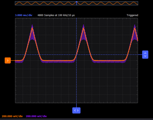
Figure 5 Current Mirror waveform
Resources:
You are to measure Iin, Rout seen into the drain of M2, the current mirror gain = Iout/Iin and determine the Norton and Thevenin equivalent circuits for this mirror.
Return to Lab Activity Table of Contents