


This version is outdated by a newer approved version. This version (11 May 2019 17:02) was approved by Doug Mercer.The Previously approved version (10 May 2019 20:15) is available.
This version (11 May 2019 17:02) was approved by Doug Mercer.The Previously approved version (10 May 2019 20:15) is available.This is an old revision of the document!
Table of Contents
Activity: Efficiency, Power Loss, and Thermal Management
Objective:
The objective of this activity is to explore the concepts of efficiency, power loss, temperature rise, and heat flow.
Notes:
As in all the ALM labs we use the following terminology when referring to the connections to the M1000 connector and configuring the hardware. The green shaded rectangles indicate connections to the M1000 analog I/O connector. The analog I/O channel pins are referred to as CA and CB. When configured to force voltage / measure current –V is added as in CA-V or when configured to force current / measure voltage –I is added as in CA-I. When a channel is configured in the high impedance mode to only measure voltage –H is added as CA-H. Scope traces are similarly referred to by channel and voltage / current. Such as CA-V , CB-V for the voltage waveforms and CA-I , CB-I for the current waveforms.
Safety:
This experiment deals with power electronics, and while the voltages are low, and power is generally less than a few watts, devices and heat sinks can get hot, and if something goes wrong, parts can fail unexpectedly. WEAR EYE PROTECTION, and DO NOT TOUCH circuits when they are running, and wait for them to cool down after shutting off power.
Background:
All electrical devices require power. A smart phone is an obvious example; it is compact, reliable (hopefully) and performs an astonishing array of functions. Electric cars, network server computers, avionics, laptop computer, and kitchen microwave oven, all require power. A common theme with most modern electronics is that powering them is not getting any easier - requirements on voltage accuracy, current capacity, size, cost, are all being pushed further and further. But no power conversion circuit is perfect, some power will be lost in the process, and it is this lost power, and what to do with it, that will be explored in this lab.
When thinking about power supplies, the term “efficiency” is often one of the first parameter that comes to mind. This is one way of comparing different power supplies, and is certainly important. But the idea of power loss is often a more practical metric to keep in the forefront of your mind. Why? Consider two laptop chargers, one is 85% efficient and the other is 90% efficient, which are typical numbers. While paying a little more for the extra bit of energy required for the 5% less efficient unit might be annoying, it's insignificant compared to what it costs to run an air conditioner (or electric oven, etc.) The real annoyance is how hot the charger gets; the 85% efficient supply dissipates 50% more power, and the temperature rise will be 1.5X as much above ambient. Have you ever left a laptop charger on your couch, and somehow a pillow found its way on top of it? That extra power makes a BIG difference!

Figure 1. Common Laptop Charger Situation
Here on Earth, there is the luxury of air to carry heat away from stuff that gets hot. What about a space application? Or even an avionic application, where air may have a fraction of its ability to move heat that it has at sea level? That's why the difference between a 99% efficient power supply and a 98% efficient supply can be tremendously important - the 98% efficient supply has double the power loss; twice as much heat must be carried away from the application, and in space, thermal radiation is the only way.
Whether the amount of power lost from a circuit is large or small, one thing is true - it WILL escape to the environment. It will escape by increasing the temperature of the circuit until the heat flowing out of the circuit is equal to the electrical power being lost, and the goal is to make sure that when this equilibrium is met, the circuit is still functioning properly.
With that in mind, let's do some experiments, and try not to burn our fingers in the process.
Materials:
ADALM1000 Active Learning Module
Or Optionally - digital multimeters, preferably with a 1A current range
Solder-less breadboard
Jumper wires
PC/Mac running LTspice and ALICE desktop tools
4 AA batteries and holder (or “battery eliminator” see Appendix)
LT3080 LDO regulator
LTM8067 Isolated Switching Regulator (on BOB)
6.2Ω, 10W power resistor
TO-220 heat sink, Aavid 7021 or similar, or various sizes of double-sided, copper-clad PCB material.
Heat sink compound / thermal grease
AD592 Temperature Sensor (soldered to extention wires
Optional: Infrared thermometer
Thermal Resistance Primer:
Why don't Linear Regulators have an efficiency number proudly displayed on the front page of the datasheet, like switching regulators? It could be because the relevant laws of physics are intuitively understood by most engineers using these parts - Current through any “black box”, multiplied by the voltage drop, equals power that will leave the box somehow. In the case of an LDO regulator, that power leaves as heat. (If the “black box” were an LED, some of that power would leave as light, if it were a motor, the power might leave as mechanical power through the rotating shaft.) And if the input supply to an LDO regulator varies widely, the efficiency will also vary widely - it could be near 100% when the input supply is just a little bit higher than the output voltage, or 10% or less, if the input is 12V and the output is 1.2V. But there are definitely situations where linear regulators are the right tool for the job. (We'll save that discussion for later.) Before even starting to build any circuitry, we know that we're going to have to get rid of some heat. The LT3080 regulator from the parts kit is in the very common T0-220 package, with a tab for mounting to a heat sink.

Figure 2. LT3080 package, pinout, thermal resistance
This shows the physical layout of the part, pinout, and three parameters, defined as follows:
TJMAX - Maximum Junction Temperature ΘJC - Thermal resistance from Junction to Case ΘJA - Thermal resistance from Junction to Ambient
Further defining terms:
Thermal Resistance - Resistance to the flow of heat, expressed as the temperature rise due to a given power flowing through the resistance.
TJ - Junction Temperature - The temperature of the “important part” of the silicon die. The junction must be kept below a certain temperature in order for the part to function properly. It is mounted to the metal tab inside the part, and encased in plastic.
TAMBIENT - Ambient Temperature - the temperature of the environment, far away from the part.
TC - Case Temperature - Temperature of the interface between the package and heat sink or printed circuit board.
These seemingly simple terms are in reality quite difficult to measure. Measuring “ambient” is not that bad; an appropriate thermometer can be used to measure the temperature of the thermal mass that the part is dumping heat into, which is often the air in the room. But what about the “case”? The case temperature is defined as the temperature of a large block of copper, to which the package is optimally mounted. It represents a theoretical minimum thermal resistance, not achievable in actual applications (for most device packages.) So while the top of the device's package is literally part of the case, a measurement of its temperature is NOT the “case temperature”.
This description from Vishay Application Note 827 illustrates this point: “For the MOSFET/heat sink assembly, a specially designed heat sink assembly of a copper block (4 in. x 4 in. x 0.75 in.) was used to simulate an infinite heat sink attached to the case of the TO-220 device.”
Junction temperature is, as the name suggests, the temperature of the operational semiconductor junction in the device, which in reality may be many junctions in a complex circuit. And it is this temperature that must be kept below the maximum specified; if exceeded, the part is not guaranteed to function properly. But note that unless your device has a built-in temperature sensor (and some do), it is difficult to measure the junction temperature directly.
Note that the maximum junction temperature can be well above the boiling point of water - too hot to touch. So using your finger to test if a circuit is cool enough is not only dangerous, it is completely inaccurate.
So how are these numbers used? The objective is to keep the junction below the maximum allowed. So we can use knowledge of how much power is dissipated in the part (near the junction), and the thermal resistance to the air, to calculate how hot the junction will get.
TJ = TAMBIENT + PD * ΘJA
Where PD is the power dissipation.
One very useful mental model is to think of thermal resistances as electrical resistances, such that:
1°C/W = 1 Ω
1W of dissipation = 1A of current being driven through the resistance
1V = 1°C temperature rise across the resistance.
Doing a quick calculation on the LT3080 in the TO-20 package, if the input voltage is 10V, output voltage is 5V, and the load current is 200mA, the power dissipated in the part is (10V - 5V) * 0.2A = 1W. This will cause a temperature rise of 40°C, so if the air in the room is 25C, the junction will heat up to approximately 65°C - well under the 125°C maximum (but hot enough to burn skin!) The electrical analogy is shown below, running a DC operating point simulation.

Figure 3. Electrical model of thermal resistance, 1W dissipation.
Notice that Tjunction is 65 “volts”, which is 65°C in the analogy. But what happens if the load current increases to 500mA? Now you have to get rid of 2.5W, which will cause a temperature rise of 100°C, pushing you right up to the maximum junction of 125°C, with no safety margin.

Figure 4. Electrical model of thermal resistance, 2.5W dissipation.
That doesn't sound like a very high performance part, and the datasheet clearly says the part is capable of delivering 1.1A of current. So what is going on, given the ΘJA of 40°C/W? Here is the key point about datasheet ΘJA numbers: ΘJA is designed to be PESSIMISTIC. That is, it is purposely measured on a circuit board, with no extra copper to spread the heat, with no extra airflow. Almost ANYTHING that you do to spread heat will effectively lower ΘJA. Table 5 illustrates this for the DD-Pak package:

Figure 5. Table 5 from LT3080 datasheet
And note that while ΘJA is listed for the TO-220 package on page 2 of the datasheet, it's not even mentioned here. Why? Because the TO-220 package is designed to be mounted to an external heat sink of some sort. It is possible to solder the back tab of the part to a circuit board, but you would normally use the DD-Pak in those situations (DD-Pak looks like a TO-220 with shorter leads and no tab.)
The LT3080 in the parts kit is the TO-220 package version, and we're not soldering it down, which means that we really ought to be using a heat sink. How does that affect our calculations? Luckily*, the heat sink manufacturer will provide the other number we need: ΘCA - the thermal resistance from case to ambient. The datasheet for the Aavid 7021 heat sink provides the following graph:
*(This is not really luck, it's an essential piece of data.)

Figure 6. Aavid 7021 Temperature rise and Thermal resistance.
This shows the following:
ΘCA is approximately 10°C/W in still air (2 Watts causes a 20°C temperature rise, from the graph).
ΘCA decreases with airflow - by quite a bit - down to about 2.25°C/W at 800ft/minute (4.06m/s)
This is reconcilable with table 5 above - the heat sink is a folded up piece of aluminum, with a total area of about 3060mm2, and a 2500mm2 PC board has a thermal resistance of about 25°C/W. But the heat sink is all aluminum, and the PC board is copper foil, but it's glued to fiberglass (a poor conductor of heat.)
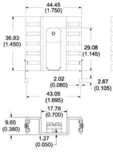
Figure 7. Aavid 7021 diagram
Let's re-run the LTspice simulation one more time, with the Aavid 7021 heat sink's thermal resistance:

Figure 8. Electrical model of thermal resistance, 2.5W dissipation with heat sink.
The expected temperature rise is about 32.5°C, for a junction temperature of 57.5°C
Procedure: LT3080 Linear Regulator
Refer to the circuit shown below.

Figure 9. LT3080 efficiency test schematic
The LTspice file should be set up to sweep the input voltage from 6V to 11V and plot input power, output power, and efficiency. Results are shown in Figure 10 below, with the red trace representing efficiency.

Figure 10. LT3080 LTspice simulation
As expected, efficiency is relatively high (about 66%) when the input voltage (shown in green) is low. As the input voltage increases, the power dissipation in the LT3080 (blue) increases, and efficiency decreases (to about 28% when the input voltage is 11V). Results of this simulation should reflect reality very accurately. The reason is that the loss mechanisms are straightforward - power dissipations are simply DC currents multiplied by DC voltages.

Figure 11. LT3080 Breadboard connections
Construct the circuit according to figure 9 on a solder-less breadboard, keeping the following in mind:
Mount the LT3080 to the heat sink first, with a small drop of heat sink compound between the package and heat sink.
Carefully twist the LT3080's leads 90 degrees such that they line up with the breadboard's columns. This is to preserve the springiness of the breadboard's contacts. Note that the “SET” resistor is a 100 KΩ resistor and a 200 KΩ resistor in series with a 50 KΩ pot. Adjust the pot for 3.3 Volts at the LT3080 output pin. The total series value of the “SET” resistor should be about 330 KΩ.
WARNING: if the SET resistors lose contact, the output voltage will increase to its maximum, and the 6.2Ω resistor will get very hot!
Also, there are options for measuring voltages and currents. Input voltage and current can be measured with digital multimeters set to appropriate voltage and current ranges. Output current can either be measured directly with a multimeter, or calculated, by first measuring the actual resistance of the load resistor with a multimeter and dividing the measured output voltage by the resistance. (The resistor in the parts kit has a 10% tolerance, so it should be measured first.) Input and output voltages and currents can also be measured with the ADALM1000 and running the Alice M1K Meter-Source tool, or with a multimeter.
Things are about to get a bit warm - too warm to touch. So we need a way of at least getting some idea of HOW warm without getting burned. The AD592 temperature sensor provides an easy way to do this:

Figure 12. AD592 Thermometer Circuit
The AD592 leads need to be extended. Longer wires can be soldered to the device pins (figure 13) and the middle lead is not connected so it can be used to provide extra support. Or the three wire female to female extension lead supplied with the ADALM1000 can be used. The TO-92 package leads are a little small for the 0.1“ square pin header connector so a small bit of masking tape placed across the leads and the connector can help stabilize the connections.


Figure 13. AD592 Connections
A small rubber band can then be used to hold the sensor against the top surface of the LT3080 as shown in Figure 14. Use a tiny drop of thermal grease between the sensor and top of the LT3080 package.

Figure 14. AD592 mounting
It was mentioned above that the top of the “case” is not truly a measurement of the case temperature - but it turns out that the temperature of the top of the case can be used to approximate the temperature of the junction - which is difficult to measure directly. Application note 834 from Vishay: describes the relationship between the measured temperature rise at the top of a package to junction temperature rise by the following formula:
Tj rise = k x Ttop rise
With typical k values of 1.18 for DDPAK package (similar to TO-220) So while we don't have actual measurements for the LT3080, we can assume that the temperature rise of the die is about 20% greater than the temperature at the top package surface, measured with an AD592, small thermocouple, or infrared thermometer.
Power up the circuit and fill out the following data table:

Note the relationship between LT3080 power dissipation, efficiency, and temperature rise.
Procedure: LTM8067 Isolated Flyback DC/DC Converter
Next, we'll explore the efficiency and thermal performance of the LTM8067 Isolated flyback module. We're not interested in the fact that it's isolated (meaning, output and input ground terminals are independent) or that it is a module (all components encased in a single package). We are interested in the fact that it is a switching converter, which is more efficient (and loses less power to the environment) than a linear regulator, at least under most circumstances. The LTM8067 in the parts kit comes mounted to a breakout board, with a potentiometer that allows the output voltage to be adjusted from 3V to 15V
.

Figure 16. LTM8067 Breakout Board
The block diagram from the datasheet shows a basic isolated flyback circuit. Without going into details, one key point is worth worth noting: unlike the pass transistor in the LT3080, The MOSFET in the LTM8067 is either off completely, or on completely, operating as a switch. This means that very little power is dissipated in the transistor. Furthermore, the resistance of the transformer windings is designed to be as small as possible, also resulting in minimal power dissipation. The Schottky diode will necessarily have some forward drop, usually about 0.4V, so that is one loss mechanism that we can predict with some accuracy. For example, if the load current is 250mA, the diode will dissipate 0.1W as heat. But that's still relatively small, compared to the dissipation in an LT3080 under some circumstances.

Figure 17. LTM8067 Block Diagram.
Setup for this experiment is straightforward; the LTM8067 BOB has four pairs of pins, and the pins of each pair are the same node. Note that with the adjustment potentiometer on the left:
* Input positive is at the top left corner
* Input ground is at the lower left corner
* Output positive is bottom center
* Output negative is top center.
Also note that the output current capability of the LTM8067 varies with input voltage as shown below:

Figure 18. LTM8067 Output Current vs. Input Voltage
Even with the BOB set to an output of 3.3V, the 6.2 Ω power resistor will draw more than 400mA, requiring about 20V input voltage. Be sure to never set the voltage of CHB output to less than 2.1 V. The current in the load resistor should always be less than 200 mA. The voltage across the resistor will be 3.3 – the voltage from CHB divided by 6.2 Ω, as below. ILOAD = (3.3 – 2.1)/6.2 = 1.2 / 6.2 = 200 mA
You could always use a second 6.2 Ω resistor in series for a total of 12.4 Ω. With a 12.4 Ω load and 3.3 V output the load current would be 3.3/12.4 or 267 mA which is still greater than the 200 mA limit but now the minimum voltage that CHB can be safely set to is 0.85 volts.

Figure 19. LTM8067 Test Schematic
Simulations of switching regulators are not as straightforward. Some aspects of the circuit's operation are modeled well - such as the control loop dynamics, and instantaneous voltages and currents. However, power loss mechanisms are not well modeled, so it is better to refer to the part's datasheet for measured results. The LTM8067 LTspice simulation is set up to show the turn-on transient waveforms by default. The green trace is the output voltage, and the red trace is input current - notice that current is drawn in “chunks” from the source, due to switching nature of the module.

Figure 20. LTM8067 Turn-on Transient
However, we can still try extracting efficiency from the LTspice simulation. Disable the startup transient SPICE directives (right-click, set to “Comment”) and enable the efficiency SPICE directives (right-click, set to “SPICE directive”). Re-run the simulation, then view the SPICE error log. Results are shown in the figure below

Figure 21. LTM8067 Efficiency(%) vs Input Voltage Simulation that MUST be Compared to Datasheet Curves
(Comparing with datasheet figure “Efficiency vs Load Current, VOUT = 3.3V” reveals that LTspice is optimistically high.)

Figure 22. LTM8067 Breadboard Circuit
Construct the circuit on a solder-less breadboard. As with the LT3080 circuit, careful construction matters.
Power up the circuit and fill out the following data table:

Note the relationship between LTM8067 power dissipation, efficiency, and temperature rise.
Questions:
How does the LTM8067 efficiency, power loss, and temperature rise compare to the LT3080? The temperature rise vs. heat dissipated curve for the Aavid heat sink is slightly curved - it appears to have a lower thermal resistance as more heat is dissipated. Why?
Resources:
* Fritzing files: efficiency_power_loss_bb
* LTSpice files: efficiency_power_loss_ltspice
Appendix
Using external wall power supply:
Shown in the figure below is a switch selectable variable supply, sometimes called a “battery eliminator”, because the voltage steps are 1.5V. The slide switch selects between six common (battery) voltages 3V, 4.5V, 6V, 7.5V, 9V, and 12V. The cost is $13.95 which is not out of the range for a student to purchase one.

Selectable regulated power supply 3-12 VDC at 1 A
Further Reading
Using .meas and .step commands to calculate efficiency in LTspice:
Return to Lab Activity Table of Contents
university/courses/alm1k/alm-power-efficiency.1557586848.txt.gz · Last modified: 11 May 2019 17:00 by Doug Mercer