 This version (08 Jan 2014 16:44) was approved by Lucian Sin.The Previously approved version (16 Nov 2012 17:38) is available.
This is an old revision of the document!
This document presents the steps to setup an environment for using the EVAL-CN0218-SDPZ evaluation board together with the Xilinx KC705 FPGA board and the Xilinx Embedded Development Kit (EDK). Below is presented a picture of the EVAL-CN0218-SDPZ Evaluation Board with the Xilinx KC705 board.
For component evaluation and performance purposes, as opposed to quick prototyping, the user is directed to use the part evaluation setup. This consists of:
The SDP-B controller board is part of Analog Devices System Demonstration Platform (SDP). It provides a high speed USB 2.0 connection from the PC to the component evaluation board. The PC runs the evaluation software. Each evaluation board, which is an SDP compatible daughter board, includes the necessary installation file required for performance testing.
Note: it is expected that the analog performance on the two platforms may differ.
Below is presented a picture of SDP-B Controller Board with the EVAL-CN0218-SDPZ Evaluation Board.
The EVAL-CN0218-SDPZ board monitors current in systems with high positive common-mode dc voltages of up to +500 V with less than 0.2% error. The load current passes through a shunt resistor, which is external to the circuit. The shunt resistor value is chosen so that the shunt voltage is approximately 500 mV at maximum load current. When using this evaluation board with the SDP board or BeMicro SDK board, apply +6 V and GND to Connector J2.
The AD7171 is a very low power 16-bit analog-to-digital converter (ADC). It contains a precision 16-bit sigma-delta (S-?) ADC and an on-chip oscillator. Consuming only 135 µA, the AD7171 is particularly suitable for portable or battery operated products where very low power is a requirement. The AD7171 also has a power-down mode in which the device consumes 5 µA, thus increasing the battery life of the product.
For ease-of-use, all the features of the AD7171 are controlled by dedicated pins. Each time a data read occurs, eight status bits are appended to the 16-bit conversion. These status bits contain a pattern sequence that can be used to confirm the validity of the serial transfer.
The output data rate of the AD7171 is 125 Hz, whereas the settling time is 24 ms. The AD7171 has one differential input and a gain of 1. This is useful in applications where the user needs to use an external amplifier to implement system-specific filtering or gain requirements.
The first objective is to ensure that you have all of the items needed and to install the software tools so that you are ready to create and run the evaluation project.
Before connecting the ADI evaluation board to the Xilinx KC705 make sure that the VADJ_FPGA voltage of the KC705 is set to 3.3V. For more details on how to change the setting for VADJ_FPGA visit the Xilinx KC705 product page.
The following commands were implemented in this version of EVAL-CN0218 reference project for Xilinx KC705 FPGA board.
| Command | Description |
|---|---|
| help? | Displays all available commands. |
| voltage? | Displays the input voltage in [mV]. |
| adcCode? | Displays the output ADC code. |
Commands can be executed using a serial terminal connected to the UART peripheral of Xilinx KC705 FPGA.
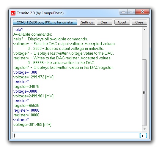
The following image shows a generic list of commands in a serial terminal connected to Xilinx KC705 FPGA's UART peripheral.

The hardware platform for each reference projects with FMC-SDP interposer and KC705 evaluation board is common. The next steps should be followed to recreate the software project of the reference design: