 This version (01 Oct 2013 16:14) was approved by Lucian Sin.The Previously approved version (11 Sep 2013 10:52) is available.
This is an old revision of the document!
This document presents the steps to setup an environment for using the EVAL-AD5542ASDZ evaluation board together with the Xilinx KC705 FPGA board and the Xilinx Embedded Development Kit (EDK). Below is presented a picture of the EVAL-AD5542ASDZ Evaluation Board with the Xilinx KC705 board.
For component evaluation and performance purposes, as opposed to quick prototyping, the user is directed to use the part evaluation setup. This consists of:
The SDP-B controller board is part of Analog Devices System Demonstration Platform (SDP). It provides a high speed USB 2.0 connection from the PC to the component evaluation board. The PC runs the evaluation software. Each evaluation board, which is an SDP compatible daughter board, includes the necessary installation file required for performance testing.
Note: it is expected that the analog performance on the two platforms may differ.
Below is presented a picture of SDP-B Controller Board with the EVAL-AD5542ASDZ Evaluation Board.
The AD5542A is a single, 16-bit, serial input, unbuffered voltage output digital-to-analog converters (DAC) that operate from a single 2.7 V to 5.5 V supply. The DAC output range extends from 0 V to VREF and is guaranteed monotonic, providing 1 LSB INL accuracy at 16 bits without adjustment over the full specified temperature range of -40°C to +85°C (AD5542A). Offering unbuffered outputs, the AD5542A achieves a 1 µs settling time with low offset errors ideal for high speed open loop control. The AD5542A incorporates a bipolar mode of operation that generates a ±VREF output swing. The AD5542A also includes Kelvin sense connections for the reference and analog ground pins to reduce layout sensitivity. The AD5542A uses a versatile 3-wire interface that is compatible with 50 MHz SPI, QSPI™, MICROWIRE™, and DSP interface standards.
The EVAL-AD5542ASDZ evaluation board is designed to help customers quickly prototype new AD5542A circuits and reduce design time.
The first objective is to ensure that you have all of the items needed and to install the software tools so that you are ready to create and run the evaluation project.
Before connecting the ADI evaluation board to the Xilinx KC705 make sure that the VADJ_FPGA voltage of the KC705 is set to 3.3V. For more details on how to change the setting for VADJ_FPGA visit the Xilinx KC705 product page.
To power on the EVAL-AD5542A evaluation board, you need to provide external +5V and -5V supply voltage to J1 connector on the board (LK8 position=B, LK9 position=A, LK7 position=A, LK3 position=B, LK2 position=A).
The following commands were implemented in this version of EVAL-AD5542A reference project for Xilinx KC705 FPGA board.
| Command | Description |
|---|---|
| help? | Displays all available commands. |
| register= | Writes to the DAC register. Accepted values: 0 .. 65535 - the value written to the DAC. |
| register? | Displays last written value in the DAC register. |
| voltage= | Sets the DAC output voltage. Accepted values: -2500 .. +2500 - desired output voltage in milivolts. |
| voltage? | Displays last written voltage value to the DAC. |
| ldacPin= | Sets the output value of LDAC pin. Accepted values: 0 - sets LDAC pin low.(default) 1 - sets LDAC pin high. |
| ldacPin? | Displays the value of LDAC pin. |
| clrPin= | Sets the output value of CLR pin. Accepted values: 0 - sets CLR pin low. 1 - sets CLR pin high.(default) |
| clrPin? | Displays the value of CLR pin. |
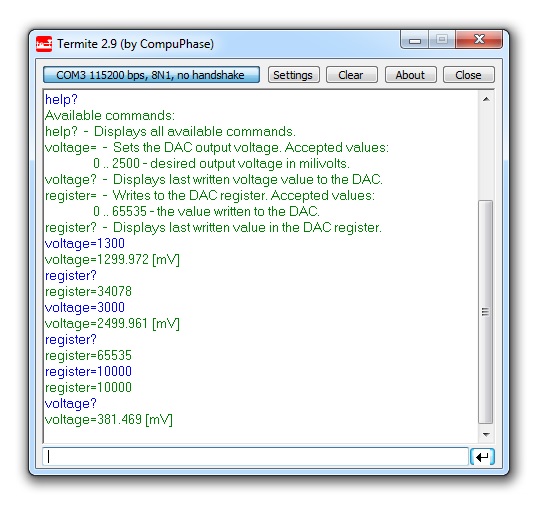
Commands can be executed using a serial terminal connected to the UART peripheral of Xilinx KC705 FPGA.
The following image shows a generic list of commands in a serial terminal connected to Xilinx KC705 FPGA's UART peripheral.

The hardware platform for each reference projects with FMC-SDP interposer and KC705 evaluation board is common. The next steps should be followed to recreate the software project of the reference design: