


This version is outdated by a newer approved version. This version (24 Feb 2022 09:21) was approved by Iulia Moldovan.The Previously approved version (11 Oct 2021 15:12) is available.
This version (24 Feb 2022 09:21) was approved by Iulia Moldovan.The Previously approved version (11 Oct 2021 15:12) is available.This is an old revision of the document!
Table of Contents
AXI_PWM_GEN
The axi_pwm_gen core is used to generate a maximum of four configurable signals(pwms). The pulses are generated according to the state of a counter, one counter for each pulse.
Features
- up to four configurable signals(period, width, offset)
- external synchronization
- external clock
The offset feature will synchronize counters 0, 1, 2 and 3 to an offset counter.
The axi_pwm_gen core can be synchronized by an external signal. The offset counter will wait for a high to low transition of the synchronization pulse. If another synchronization is needed, the external_sync signal should be set high and the load_config should be toggled(by register write). This will cause the counters to wait for another external_sync high to low transition. To disable a pwm, write 0 to it's period register.
Block Diagram

Configuration Parameters
| Name | Description | Default Value |
|---|---|---|
ID | Core ID should be unique for each IP in the system | 0 |
ASYNC_CLK_EN | Use external clock, asynchronous to s_axi_aclk | 1 |
N_PWMS | Number of pulses/pwms | 1 |
PWM_EXT_SYNC | PWM offset counter uses external sync | 0 |
EXT_ASYNC_SYNC | The external sync for pulse 0 is asynchronous | 0 |
PULSE_0_WIDTH | Pulse 0 width (number of clk cycles) | 7 |
PULSE_1_WIDTH | Pulse 1 width (number of clk cycles) | 7 |
PULSE_2_WIDTH | Pulse 2 width (number of clk cycles) | 7 |
PULSE_3_WIDTH | Pulse 3 width (number of clk cycles) | 7 |
PULSE_0_PERIOD | Pulse 0 period (number of clk cycles) | 10 |
PULSE_1_PERIOD | Pulse 1 period (number of clk cycles) | 10 |
PULSE_2_PERIOD | Pulse 2 period (number of clk cycles) | 10 |
PULSE_3_PERIOD | Pulse 3 period (number of clk cycles) | 10 |
PULSE_0_OFFSET | Pulse 1 period (number of clk cycles) | 0 |
PULSE_1_OFFSET | Pulse 1 period (number of clk cycles) | 0 |
PULSE_2_OFFSET | Pulse 2 period (number of clk cycles) | 0 |
PULSE_3_OFFSET | Pulse 3 period (number of clk cycles) | 0 |
Signal and Interface Pins
| Interface | Pin | Type | Description |
|---|---|---|---|
External clock | Clock signal | ||
ext_clk | input | Input clock | |
External sync | external sync signal | ||
external_sync, | input | Synchronize pulses to an external signal | |
PWM | pwm signals | ||
pwm_0 | output [1] | Output pwm 0 | |
pwm_1 | output [1] | Output pwm 1 | |
pwm_2 | output [1] | Output pwm 2 | |
pwm_3 | output [1] | Output pwm 3 | |
s_axi | AXI Memory Map interface | ||
Functionality
The axi_pwm_gen offers the possibility of four output signals(pwms). Pulse 0, 1, 2 and 3 can have offsets in referenced to pwm counter.
The pulse generator is based on incrementing counters. In a pulse period, the first interval of the signal, until the level transition, the signal level is high(pulse_width) and the second interval is low(pulse_period-pulse_width).
By default, all counters start at the same time. When a different phase(delay) is needed between the pulses, the offset value is calculated in number of clock cycles:
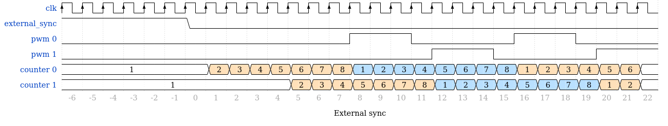
The below timing diagram, shows the external_sync functionality.
The below timing diagram, shows the load_config functionality. All four pulses are active and all four pulses have the same period.

Register map
| Address | Bits | Name | Type | Default | Description | |
| DWORD | BYTE | |||||
| 0x0000 | 0x0000 | REG_VERSION | Version and Scratch Registers | |||
|---|---|---|---|---|---|---|
| [31:0] | VERSION[31:0] | RO | 0x00010100 | Version number. Unique to all cores. | ||
| 0x0001 | 0x0004 | REG_ID | Core ID | |||
| [31:0] | ID[31:0] | RO | 0x00000000 | Instance identifier number. | ||
| 0x0002 | 0x0008 | REG_SCRATCH | Version and Scratch Registers | |||
| [31:0] | SCRATCH[31:0] | RW | 0x00000000 | Scratch register. | ||
| 0x0003 | 0x000c | REG_CORE_MAGIC | Identification number | |||
| [31:0] | SCRATCH[31:0] | RW | 0x504C5347 | Identification number. | ||
| 0x0004 | 0x0010 | REG_RSTN | Reset and load values | |||
| [1] | LOAD_CONFIG | WO | 0x0 | Loads the new values written in the config registers. | ||
| [0] | RESET | RW | 0x0 | Reset, default is (0x0). | ||
| 0x0005 | 0x0014 | REG_N_PULSES | Number of pulses. | |||
| [31:0] | RO | 0x0000 | Number of configurable pulses. | |||
| 0x0010 | 0x0040 | REG_PULSE_0_PERIOD | Pulse 0 period. | |||
| [31:0] | PULSE_0_PERIOD[31:0] | RW | 0x0000 | Pulse 0 duration defined in number of clock cycles. | ||
| 0x0011 | 0x0044 | REG_PULSE_0_WIDTH | Pulse 0 width. | |||
| [31:0] | PULSE_0_WIDTH[31:0] | RW | 0x0000 | Pulse 0 width(high time) defined in number of clock cycles. | ||
| 0x0012 | 0x0048 | REG_PULSE_0_OFFSET | Pulse 0 offset. | |||
| [31:0] | PULSE_0_OFFSET[31:0] | RW | 0x0000 | Pulse 0 offset, defined in number of clock cycles. | ||
| 0x0013 | 0x004c | REG_PULSE_1_PERIOD | Pulse 1 period. | |||
| [31:0] | PULSE_1_PERIOD[31:0] | RW | 0x0000 | Pulse 1 duration, defined in number of clock cycles. | ||
| 0x0014 | 0x0050 | REG_PULSE_1_WIDTH | Pulse 1 width. | |||
| [31:0] | PULSE_1_WIDTH[31:0] | RW | 0x0000 | Pulse 1 width(high time), defined in number of clock cycles. | ||
| 0x0015 | 0x0054 | REG_PULSE_1_OFFSET | Pulse 1 offset. | |||
| [31:0] | PULSE_1_OFFSET[31:0] | RW | 0x0000 | Pulse 1 offset, defined in number of clock cycles. | ||
| 0x0016 | 0x0058 | REG_PULSE_2_PERIOD | Pulse 2 period. | |||
| [31:0] | PULSE_2_PERIOD[31:0] | RW | 0x0000 | Pulse 2 duration, defined in number of clock cycles. | ||
| 0x0017 | 0x005c | REG_PULSE_2_WIDTH | Pulse 2 width. | |||
| [31:0] | PULSE_2_WIDTH[31:0] | RW | 0x0000 | Pulse 2 width(high time) defined in number of clock cycles. | ||
| 0x0018 | 0x0060 | REG_PULSE_2_OFFSET | Pulse 2 offset. | |||
| [31:0] | PULSE_2_OFFSET[31:0] | RW | 0x0000 | Pulse 2 offset. | ||
| 0x0019 | 0x0064 | REG_PULSE_3_PERIOD | Pulse 3 period. | |||
| [31:0] | PULSE_3_PERIOD[31:0] | RW | 0x0000 | Pulse 3 duration. | ||
| 0x001a | 0x0068 | REG_PULSE_3_WIDTH | Pulse 3 width. | |||
| [31:0] | PULSE_3_WIDTH[31:0] | RW | 0x0000 | Pulse 3 width(high time). | ||
| 0x001b | 0x006c | REG_PULSE_3_OFFSET | Pulse 3 offset. | |||
| [31:0] | PULSE_3_OFFSET[31:0] | RW | 0x0000 | Pulse 3 offset. | ||
| Tue Mar 30 10:21:25 2021 | ||||||
Navigation - HDL User Guide
resources/fpga/docs/axi_pwm_gen.1634112427.txt.gz · Last modified: 13 Oct 2021 10:07 by Iulia Moldovan