


This version is outdated by a newer approved version. This version (12 Nov 2019 19:31) was approved by Paul Kern.The Previously approved version (12 Nov 2019 19:20) is available.
This version (12 Nov 2019 19:31) was approved by Paul Kern.The Previously approved version (12 Nov 2019 19:20) is available.This is an old revision of the document!
Table of Contents
ADIS1650x-x/PCBZ BREAKOUT BOARD WIKI GUIDE
OVERVIEW
There are seven (7) breakout boards that support ADIS1650x IMU products. These breakout boards that provide a simple way to develop a prototype connection between the ADIS1650x IMUs and an existing embedded processor platform. This breakout board already contains the ADIS1650x IMU and one 16-pin header, which mates to 2 mm ribbon cables. As a general guideline, these breakout boards will support reliable communications over ribbon cables that are up to 20 cm in length, but it is always a good idea to validate signal integrity before relying on this type of connection to support a critical communication link.


PART NUMBER SUMMARY
Please see the follow table for a list of available breakout boards, along with the IMU model number that is on each board.
| MODEL NUMBERS | MEASUREMENT RANGE | ||
|---|---|---|---|
| BREAKOUT BOARD | IMU | GYROSCOPE | ACCELEROMETER |
| ADIS16500/PCBZ | ADIS16500AMLZ | +/-2000 dps | +/-40g |
| ADIS16505-1/PCBZ | ADIS16505-1BMLZ | +/-125 dps | +/-8g |
| ADIS16505-2/PCBZ | ADIS16505-2BMLZ | +/-500 dps | +/-8g |
| ADIS16505-3/PCBZ | ADIS16505-3BMLZ | +/-2000 dps | +/-8g |
| ADIS16507-1/PCBZ | ADIS16507-1BMLZ | +/-125 dps | +/-40g |
| ADIS16507-2/PCBZ | ADIS16507-2BMLZ | +/-500 dps | +/-40g |
| ADIS16507-3/PCBZ | ADIS16507-3BMLZ | +/-2000 dps | +/-40g |
The primary attributes that differentiate each of these models are measurement range (gyroscopes and accelerometers) and the calibration temperature range.
EVAL-ADIS2 CONNECTION
The J1 connector on each ADIS1650x-x/PCBZ breakout board is pin-for-pin compatible with the same connector (J1) on the EVAL-ADIS2 evaluation system. The picture below shows the EVAL-ADIS2 connectors.
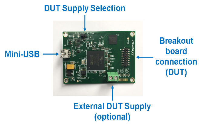
If connecting an external power supply, refer to the picture below for the polarity of the J3 external power connector:

The user should follow these steps when connecting the xxx to the EVAL-ADIS2 evaluation system:
1. Ensure that Jumper JP1 is straddling the left “+3.3V REG” pin and the center pin, assuming the EVAL-ADIS2 board is oriented with the Mini-USB connector is on the left-hand side.
Note: If the user wishes to use an external power supply, move the JP1 jumper so that it straddles the center and lower pin and connect the external supply to Connector J3. GND is the left pin and VDD (+3.3 V) is the right pin.
2. Connect the ribbon cable between the EVAL-ADIS2 and ADIS1650x-x evaluation board.
3. Install the SDP Drivers from EVAL-ADIS2 USB Drivers.
3. Install the ADIS-EVAL2 Evaluation software from EVAL-ADIS2 Evaluation Software
4. Connect the EVAL-ADIS2 USB cable to the PC and verify that LED1 and LED2 are illuminated on the EVAL-ADIS2 board.

5. More information regarding the EVAL-ADIS2 evaluation system can be found at: EVAL-ADIS2 Wiki Guide
6. More information regarding the operation of the evaluation software can be found at: adis1650x_evalguide_pr.c.pdf
DIMENSTIONS/MOUNTING HOLES
These breakout boards have four mounting holes (one in each corner) which support attachment to another surface with M2 machine screws. Please see the following diagram for more details:

INTERFACE CONNECTOR
Please see the following table for the pin assignments for the interface connector (J1)
| PIN | NAME | DESCRIPTION |
|---|---|---|
| 1 | ~RST | Reset, Active Low |
| 2 | SCLK | Serial Clock (Serial Peripheral Interface) |
| 3 | ~CS | Chip Select (Serial Peripheral Interface), Active Low |
| 4 | DOUT | Data Output (Serial Peripheral Interface) |
| 5 | DNC | Do not connect |
| 6 | DIN | Data Input (Serial Peripheral Interface) |
| 7 | GND | Ground |
| 8 | GND | Ground |
| 9 | GND | Ground |
| 10 | VDD | Power Supply, +3.3V |
| 11 | VDD | Power Supply, +3.3V |
| 12 | VDD | Power Supply, +3.3V |
| 13 | DR | Data Ready |
| 14 | SYNC | Sync Input |
| 15 | DNC | Do not connect |
| 16 | DNC | Do not connect |
CABLING
J1 supports connection with the following style of cables: 2.00 mm IDC Ribbon Cable Assembly
TIP: Use “2.00 mm IDC Ribbon Cable Assembly” as search criteria to find the latest options on the market.
At the time of initial release for these breakout boards, we were most familiar with the TCSD Series from Samtec.
ELECTRICAL SCHEMATIC
The following diagram illustrates the electrical schematic for the ADIS16500/PCBZ. Please note that the only difference in the other models will be in the IMU (ADIS16470AMLZ is shown in the following view). Click on this image to access a higher-resolution view.

REFERENCE DESIGNS & CODE EXAMPLES
This section provides a list of reference designs for those who are ready to evaluate the ADIS1650x. These references designs include one or both of the following:
- The physical connection between the ADIS1647x-x/PCB and a specific embedded processor platform/system
- Embedded code that lists all ADIS1650x user registers, manages the ADIS1650x's SPI protocol requirements, and provides examples for accessing the ADIS1650x's registers
resources/eval/user-guides/inertial-mems/imu/adis1650x-pcb.1573583467.txt.gz · Last modified: 12 Nov 2019 19:31 by Paul Kern